
Determining equivalent waveforms for distorted waveforms

a technology of equivalent waveforms and distorted waveforms, applied in error detection/correction, program control, instruments, etc., can solve the problems of clock frequency, timing and signal integrity errors, and the source of device geometry and desired power consumption, so as to achieve accurate equivalent waveforms and obtain them quickly

Active Publication Date: 2007-09-18
SYNOPSYS INC
View PDF4 Cites 8 Cited by
  • Summary
  • Abstract
  • Description
  • Claims
  • Application Information

AI Technical Summary

Problems solved by technology

Timing and signal integrity are ever increasingly important issues in integrated circuit design, particularly due to the increase in clock frequency, chip size and the decrease in device geometry and desired power consumption.
One of the most common sources of timing and signal integrity errors is crosstalk, which is mainly due to the capacitive coupling of adjacent conductors.
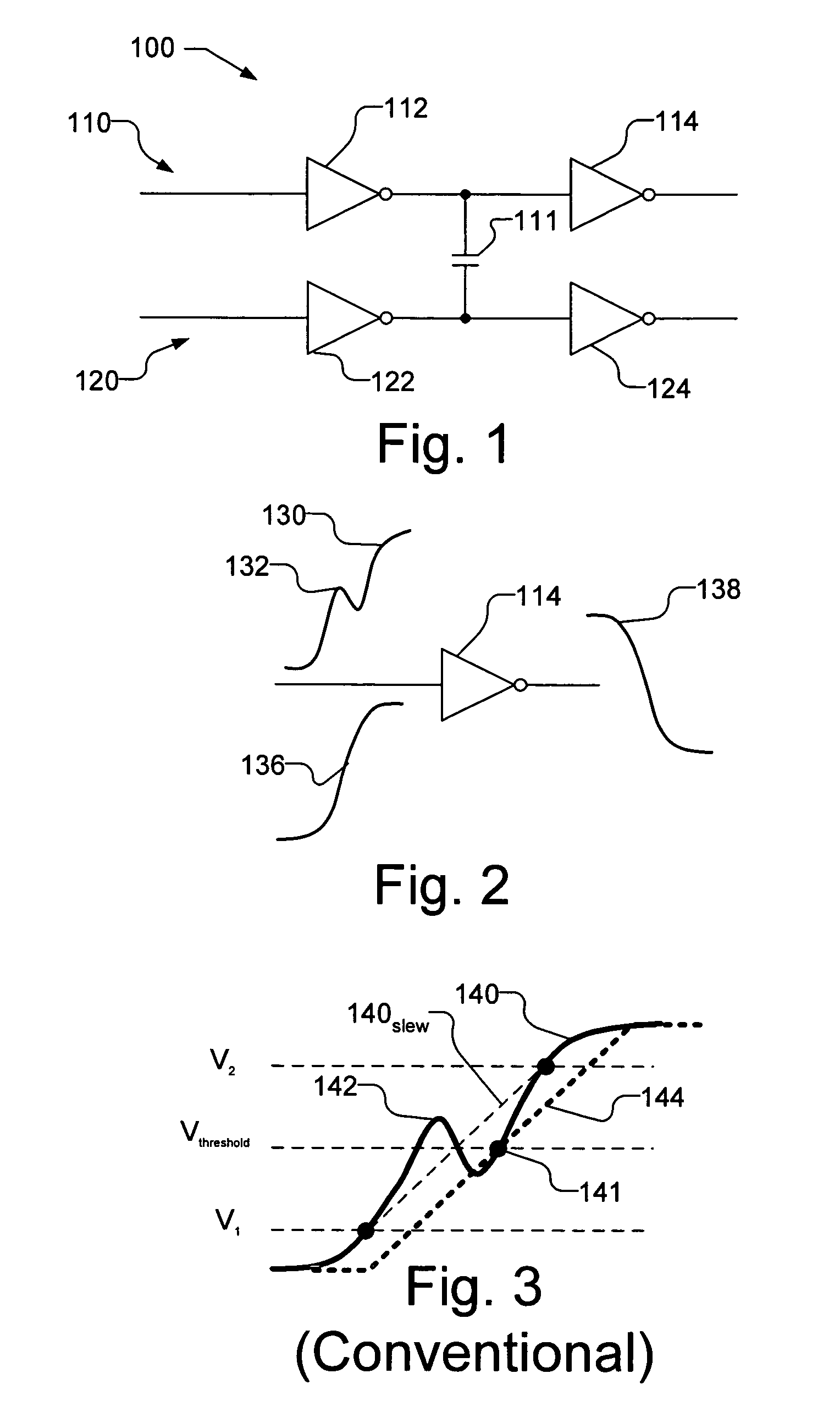
Crosstalk generally causes a distortion in the waveform of an input signal, which may result in incorrect logic transition, e.g., a gate may switch at an incorrect time, or delay variations on a signal line.
The delay variation may propagate downstream and cause a timing violation in other parts of the circuit.

Method used


Image

  • Determining equivalent waveforms for distorted waveforms
  • Determining equivalent waveforms for distorted waveforms
  • Determining equivalent waveforms for distorted waveforms

Examples


Embodiment Construction

[0020]FIG. 1 schematically illustrates an example of a cross coupled circuit 100 that may have its timing analyzed using an equivalent waveform that is produced in accordance with an embodiment of the present invention. The cross coupled circuit 100 includes a primary line 110 that is coupled to an aggressor line 120 through cross coupling capacitance, shown as capacitor 111. The primary line 110 is illustrated as including an inverter 112 coupled to a second inverter 114 and the aggressor line 120 is similarly illustrated as an inverter 122 coupled to a second inverter 124. It should be understood that the cross coupled circuit 100 is merely exemplary and that the present invention may be used advantageously with any circuit that suffers from waveform distortion due to various reasons including, but not limited to, capacitive coupling, inductive coupling, inductive ringing, and resistive shielding effects.

[0021]Generally, each node in the cross coupled circuit 100 includes a self-c...


PUM


Abstract

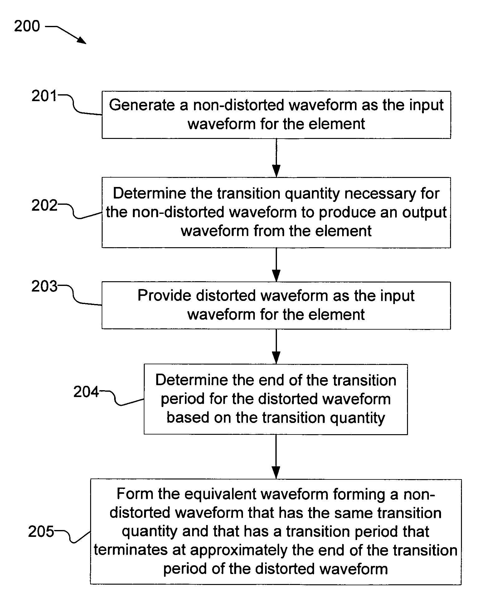
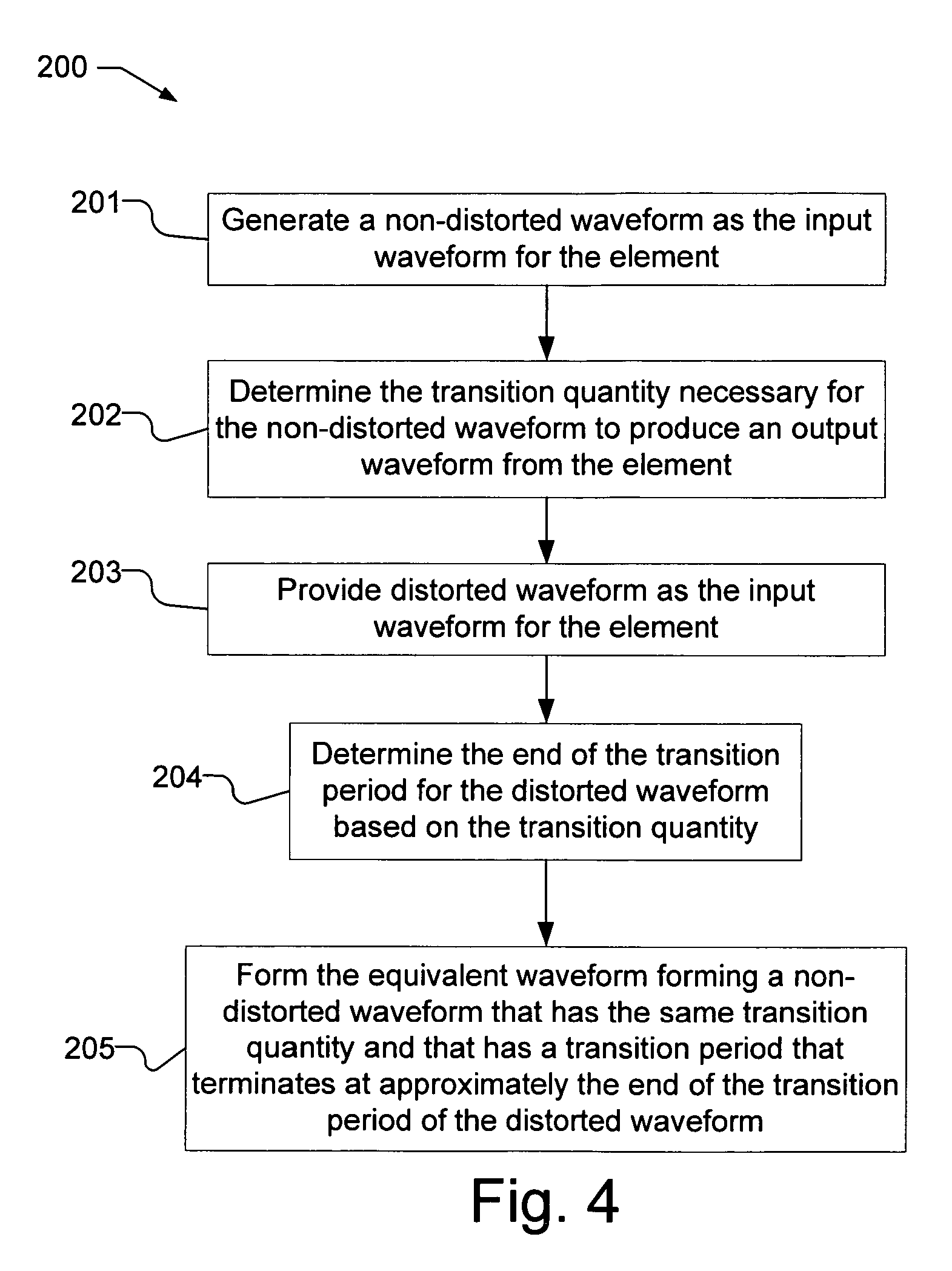
An equivalent waveform for a distorted waveform used in timing and signal integrity analysis in the design of an integrated circuit is automatically generated. The equivalent waveform is produced by calculating the transition quantity of a first non-distorted waveform. The transition quantity is the amount of transition of the first non-distorted waveform that is required for the cell to produce an output waveform with a predetermined end voltage. The end point of the transition period for the distorted waveform is then determined based on when the distorted waveform has accumulated the same transition quantity. The equivalent waveform can then be formed by computing a second non-distorted waveform such that the end point of the transition period for the second non-distorted waveform coincides with the end point of the transition period for the distorted waveform.

Description

BACKGROUND[0001]1. Field of the Invention[0002]The present invention relates to the design of semiconductor chips. More specifically, the present invention relates to a method and an apparatus for generating equivalent waveforms used in timing analysis and in signal integrity analysis for an integrated circuit design.[0003]2. Related Art[0004]Timing and signal integrity are ever increasingly important issues in integrated circuit design, particularly due to the increase in clock frequency, chip size and the decrease in device geometry and desired power consumption. Timing analysis, such as static timing analysis, is used to verify, and aid in the correction of chip timing problems. In general, static timing analysis compares the worst case timing of all possible paths between an input signal and an output signal to a preset criterion. Timing analysis is typically performed at the transistor or cell level using libraries of information, such as delay and slew, based on simple input w...

Claims


Application Information

Patent Timeline
Patent Type & Authority Patents(United States)
IPC IPC(8): G06F17/50
CPCG06F17/5031G06F17/5036G06F30/3312G06F30/367
Inventor DING, LITEHRANI, PEIVAND FALLAHKASNAVI, ALIREZA
Owner SYNOPSYS INC
Learn More