

Semiconductor integrated circuit having multi-level interconnection, CAD method and CAD tool for designing the semiconductor integrated circuit
a semiconductor integrated circuit and multi-level interconnection technology, applied in logic circuit coupling/interface arrangement, pulse technique, instruments, etc., can solve the problems of high current dissipation in power supply wiring, difficult addition of such supplemental power supply wiring, and inevitable redesign of layou
- Summary
- Abstract
- Description
- Claims
- Application Information
AI Technical Summary
Benefits of technology
Problems solved by technology
Method used
Image

Examples
first embodiment
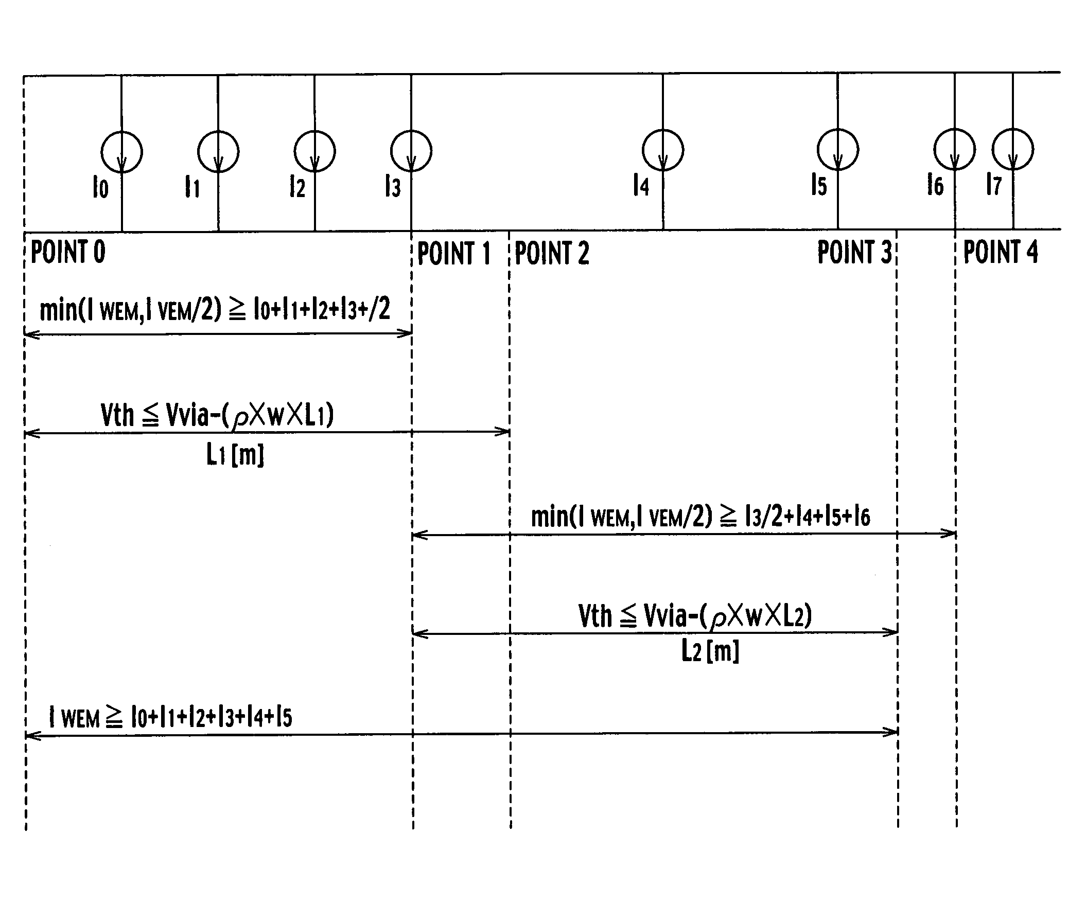
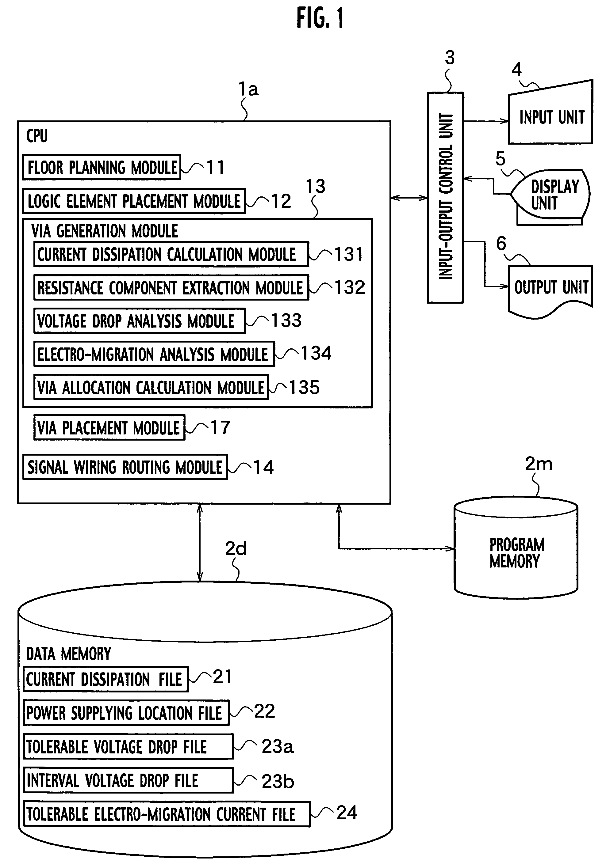
[0049]As shown in FIG. 1, a designing tool according to a first embodiment of the present invention is a computer system encompassing a input unit 4 configured to accept input data and instructions from an operator, a central processing unit (CPU) la configured to control and perform various operations of layout design, etc., an output unit 6 configured to provide layout results, etc., a display unit 5 configured to display input data, intermediate data and output data including the result of layout design, a data memory 2d configured to store various data necessary for layout design of a semiconductor integrated circuit, etc. and a program memory 2m configured to store layout design program of a semiconductor integrated circuit, etc.
[0050]The designing tool of the first embodiment further encompasses an input / output control unit 3. Through the input / output control unit 3, the input unit 4, the output unit 6 and the display unit 5 are connected to the CPU 1a.
[0051]The CPU 1a has a ...
second embodiment
[0138]As shown in FIG. 14, a designing tool according to a second embodiment of the present invention is a computer system encompassing an input unit 4 configured to accept input data and instructions from an operator, a CPU 1b configured to control and perform various operations of layout design, etc, an output unit 6 configured to provide layout results, etc. and display unit 5 configured to display input data, intermediate data and output data including the result of layout design a data memory 2d configured to store various data necessary for layout design of a semiconductor integrated circuit, etc. and a program memory 2m configured to store layout design program of a semiconductor integrated circuit, etc.
[0139]The designing tool of the second embodiment further encompasses an input / output control unit 3. Through the input / output control unit 3, the input unit 4, the output unit 6 and the display unit 5 are connected to the CPU 1b.
[0140]The CPU 1b of the designing tool accordi...
third embodiment
[0172]As shown in FIG. 19, a designing tool according to a first embodiment of the present invention is a computer system encompassing: an input unit 4 configured to accept input data and instructions from an operator, a CPU 1c configured to control and perform various operations of layout design, etc., an output unit 6 configured to provide layout results, etc., a display unit 5 configured to display input data, intermediate data and output data including the result of layout design, a data memory 2d configured to store various data necessary for layout design of a semiconductor integrated circuit, etc. and a program memory 2m configured to store layout design program of a semiconductor integrated circuit, etc. The designing tool of the first embodiment further encompasses an input / output control unit 3. Through the input / output control unit 3, the input unit 4, the output unit 6 and the display unit 5 are connected to the CPU 1c.
[0173]The CPU 1c provided in the designing tool of ...
PUM
 Abstract
Description
Claims
Application Information