

Method for regeneration of an electrolysis bath for the production of a compound I-III-VI2 in thin layers
a technology of iiivi2 and thin film, applied in the direction of electrolysis process, electrolysis inorganic material coating, electrolysis components, etc., can solve the problems of difficult to adapt to industrial scale, difficult to control the quality of electrodeposited precursors, and require very expensive vacuum equipment and precursor targets, etc., to achieve the effect of regenerating the electrolysis bath
- Summary
- Abstract
- Description
- Claims
- Application Information
AI Technical Summary
Benefits of technology
Problems solved by technology
Method used
Image

Examples
Embodiment Construction
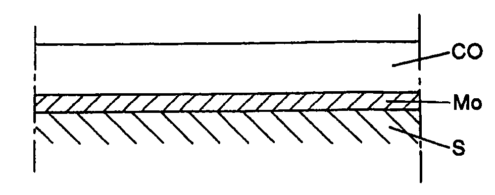
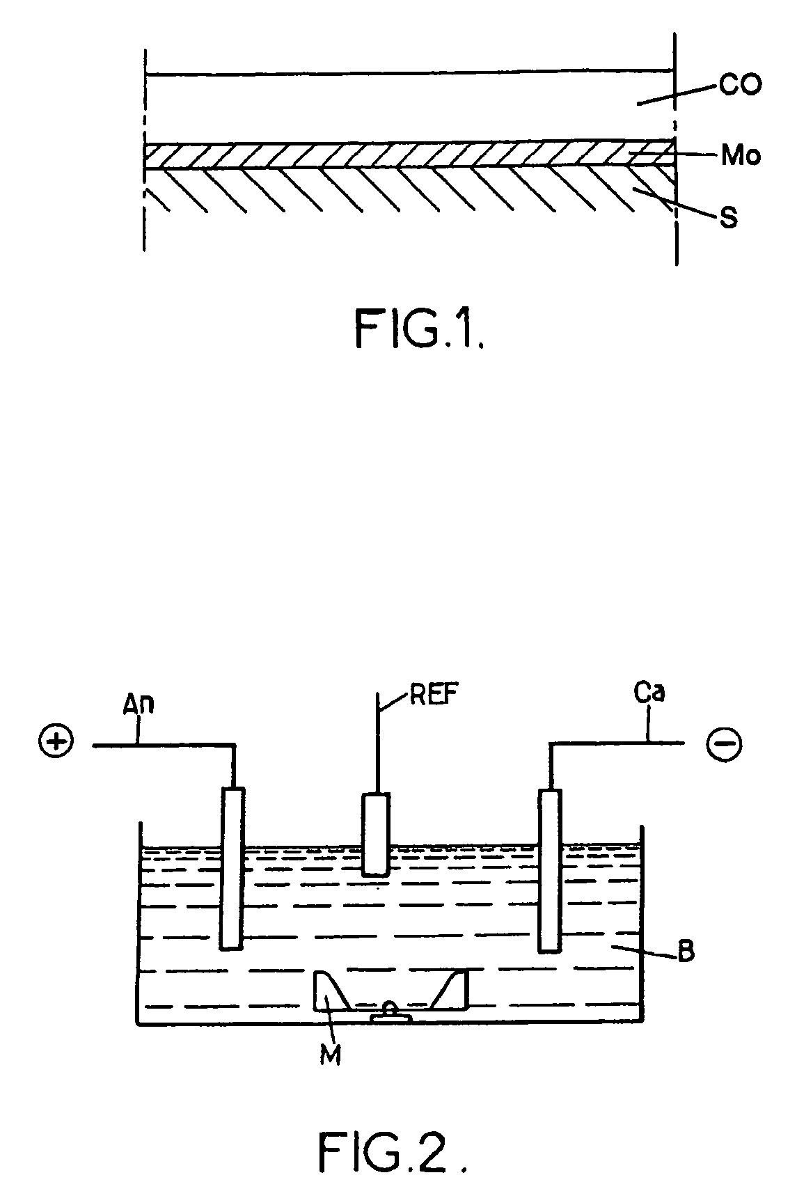
[0032]Referring to FIG. 1, copper indium diselenide films CO are obtained at room pressure and room temperature by electrodeposition of a thin precursor film of suitable composition and suitable morphology on a glass substrate S coated with molybdenum Mo. The term “precursor film” is understood to mean a thin layer of overall composition close to CuInSe2 and obtained directly after deposition by electrolysis, without any subsequent treatment.
[0033]The electrodeposition is carried out using an acid bath B (FIG. 2), stirred by blades M, which contains an indium salt, a copper salt and selenium oxide in solution. The concentrations of these precursor elements are between 10−4 and 10−2 M. The pH of the solution is set between 1 and 4.
[0034]Three electrodes, An, Ca and REF, including:[0035]a molybdenum electrode Ca (standing for cathode) on which the thin film forms by electrodeposition; and[0036]a mercurous sulfate reference electrode REF, are immersed in the bath B.
[0037]The electrical...
PUM
| Property | Measurement | Unit |
|---|---|---|
| electrical potential | aaaaa | aaaaa |
| electrical potential | aaaaa | aaaaa |
| thickness | aaaaa | aaaaa |
Abstract
Description
Claims
Application Information