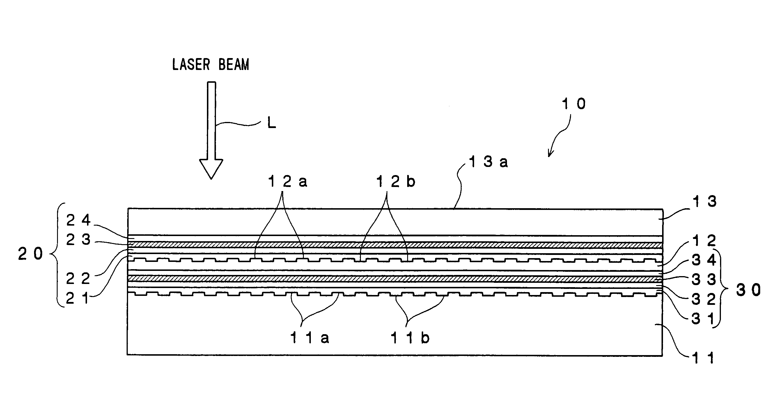
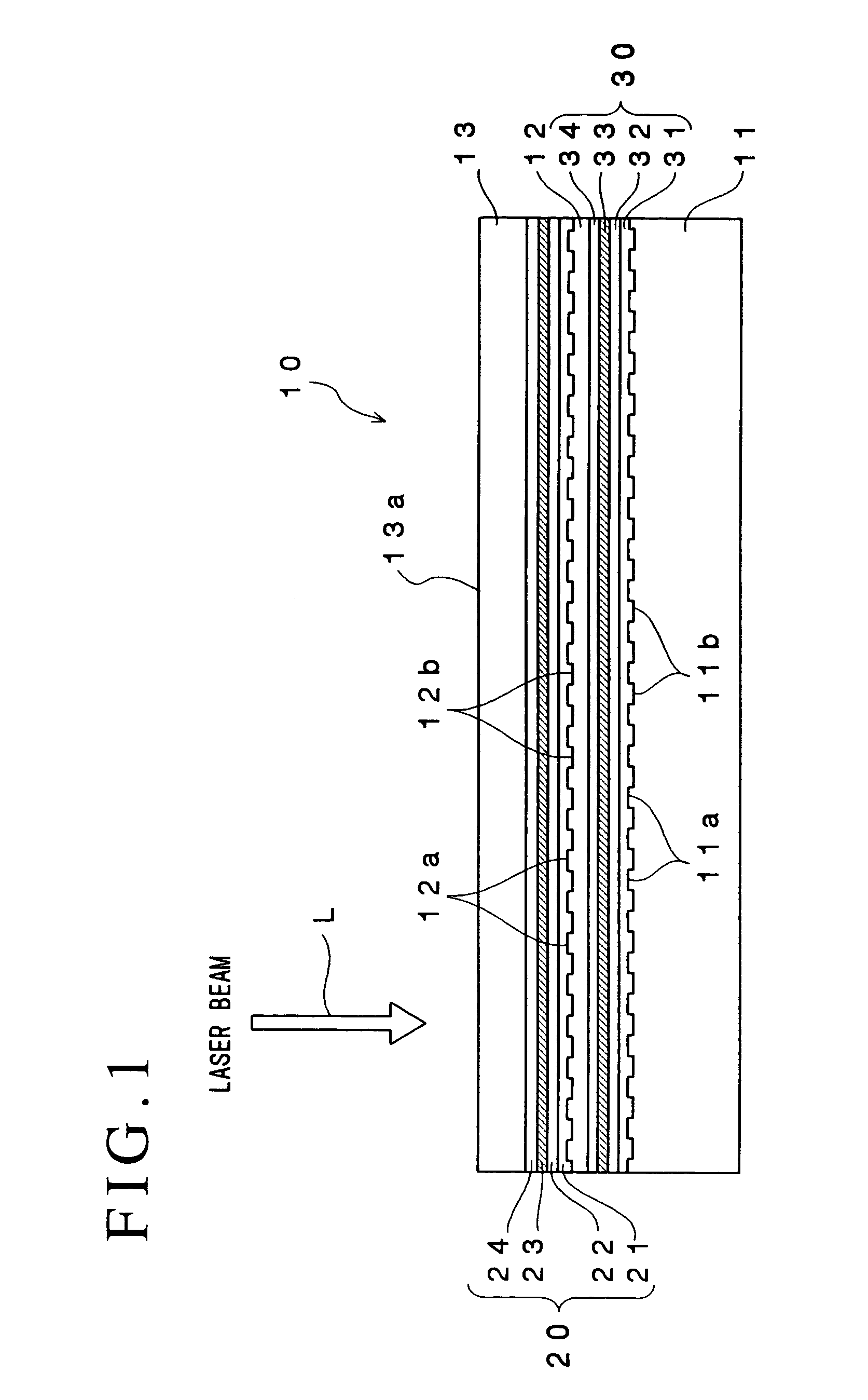
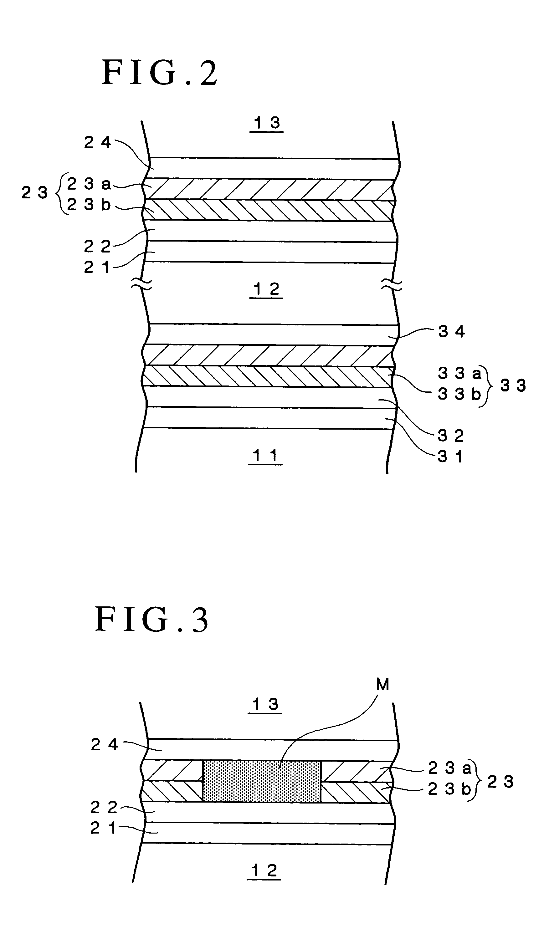
Optical recording medium and method for recording and reproducing data
a technology of optical recording medium and data, which is applied in the direction of flat record carrier container, instruments, thermography, etc., can solve the problems that the data recorded in the lb>1/b> layer cannot be reproduced in a desired manner, and achieve the effects of improving the recording characteristic and reproducing characteristic, high light transmittance, and high thermal conductivity
- Summary
- Abstract
- Description
- Claims
- Application Information
AI Technical Summary
Benefits of technology
Problems solved by technology
Method used
Image

Examples
working examples
[0127]Hereinafter, working examples will be set out in order to further clarify the advantages of the present invention.
working example 1
[0128]An optical recording medium sample #1 was fabricated in the following manner.
[0129]A disk-like polycarbonate substrate having a thickness of 1.1 mm and a diameter of 120 mm and formed with grooves and lands on the surface thereof was first fabricated by an injection molding process so that the track pitch (groove pitch) was equal to 0.32 μm.
[0130]Then, the polycarbonate substrate was set on a sputtering apparatus and a reflective film consisting of an alloy of Ag, Pd and Cu and having a thickness of 100 nm, a fourth dielectric film containing a mixture of ZnS and SiO2 and having a thickness of 40 nm, a second L1 recording film containing Cu as a primary component and having a thickness of 3 nm, a first L1 recording film containing Si as a primary component and having a thickness of 3 nm and a third dielectric film containing the mixture of ZnS and SiO2 and having a thickness of 22 nm were sequentially formed on the surface of the polycarbonate substrate on which the grooves an...
working example 2
[0153]An optical recording medium sample #4 was fabricated in the following manner.
[0154]A disk-like polycarbonate substrate having a thickness of 1.1 mm and a diameter of 120 mm and formed with grooves and lands on the surface thereof was first fabricated by an injection molding process so that the track pitch (groove pitch) was equal to 0.32 μm.
[0155]Then, the polycarbonate substrate was set on a sputtering apparatus and a reflective film consisting of an alloy of Ag, Pd and Cu and having a thickness of 8 nm, a second dielectric film containing a mixture of ZnS and SiO2 and having a thickness of 28 nm, a second recording film containing Cu as a primary component and having a thickness of 5 nm, a first recording film containing Si as a primary component and having a thickness of 5 nm and a first dielectric film containing the mixture of ZnS and SiO2 and having a thickness of 22 nm were sequentially formed on the surface of the polycarbonate substrate on which the grooves and lands ...
PUM
| Property | Measurement | Unit |
|---|---|---|
| thickness | aaaaa | aaaaa |
| wavelength | aaaaa | aaaaa |
| light transmittance | aaaaa | aaaaa |
Abstract
Description
Claims
Application Information
 - R&D
- Intellectual Property
- Life Sciences
- Materials
- Tech Scout
- Unparalleled Data Quality
- Higher Quality Content
- 60% Fewer Hallucinations
Browse by: Latest US Patents, China's latest patents, Technical Efficacy Thesaurus, Application Domain, Technology Topic, Popular Technical Reports.
© 2025 PatSnap. All rights reserved.Legal|Privacy policy|Modern Slavery Act Transparency Statement|Sitemap|About US| Contact US: help@patsnap.com