Printed circuit board including embedded resistor and method of fabricating the same

a technology of printed circuit boards and resistors, which is applied in the direction of printed resistor incorporation, resistor details, and printed element electric connection formation, etc., can solve the problems of reducing the reliability of final goods, copper terminals, and easy oxidation to external environments

Inactive Publication Date: 2007-10-02
SAMSUNG ELECTRO MECHANICS CO LTD
View PDF9 Cites 34 Cited by
  • Summary
  • Abstract
  • Description
  • Claims
  • Application Information

AI Technical Summary

Benefits of technology

[0041]Therefore, the present invention has been made keeping in mind the above disadvantages occurring in the prior arts, and an object of the present invention is to provide a PCB including embedded resistors, which assures consistency of resistance values of the embedded resistors, and a method of fabricating the same.
[0042]Another object of the present invention is to provide a PCB including embedded resistors in high density, in which the number of embedded resistors per unit area can increase, and a method of fabricating the same.
[0043]A further object of the present invention is to provide a PCB including embedded resistors, in which a length or a sectional area of each embedded resistor is easily controlled, and a method of fabricating the same.

Problems solved by technology

The conventional PCB including the embedded resistor fabricated through the above procedure of FIGS. 1a to 1c is problematic in that the copper terminals 12, 12′ exposed to external environments are readily oxidized because of a process delay between steps of FIGS. 1b and 1c.
Another problem is that if a solder mask liquid 16 is coated on the oxidized copper terminals 12, 12′ in a subsequent process, the oxidation of the copper terminals 12, 12′ is promoted.
Additionally, when a resistor paste is coated on a panel having a size of about 50×60 cm usually employed in the course of fabricating PCBs, a nonuniform thickness of the thick film resistor 15 leads to inconsistent resistance values, thereby reducing the reliability of final goods.
However, the PCB including the embedded resistor of FIGS. 2a to 2f is problematic in that since the resistor paste is coated through a screen printing process, the thickness of the resistor paste is nonuniform.
Another problem is that since the laser trimming process must be carried out for every embedded resistor to adjust the resistance value of the embedded resistor, the working speed is slow, resulting in significantly reduced productivity.
However, the PCB including the embedded resistor of FIGS. 3a to 3f is problematic in that since the resistor is formed perpendicular to the PCB, when a resistor having a high resistance value is needed, it is difficult to increase a length of the embedded resistor or reduce a sectional area of the hole (a).
Furthermore, the PCB is problematic in that a limit of the resistance value of the embedded resistor restricts the freedom in designing the PCB, and thus, it is difficult to realize miniaturization and sophisticated functions of final electronic goods.

Method used


Image

  • Printed circuit board including embedded resistor and method of fabricating the same
  • Printed circuit board including embedded resistor and method of fabricating the same
  • Printed circuit board including embedded resistor and method of fabricating the same

Examples


first embodiment

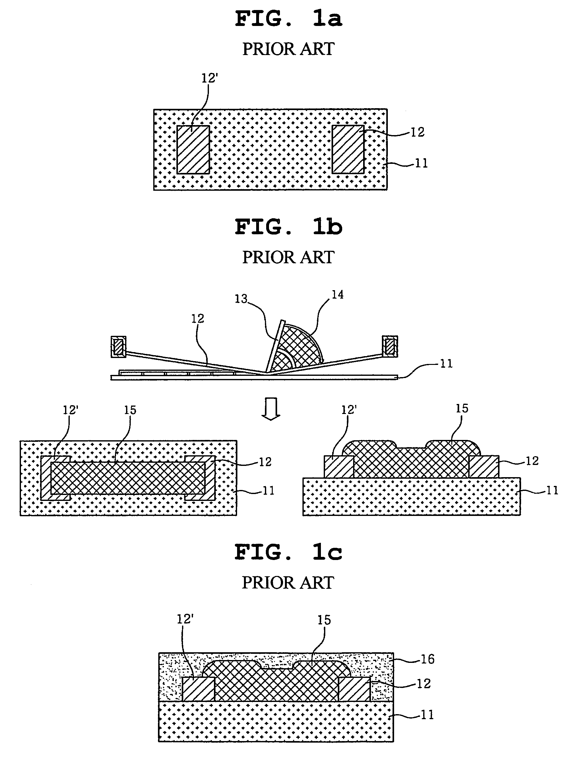
[0094]As shown in FIG. 4h, the dry film 160, 160′ coated on upper and lower sides of the substrate 110 is removed using a stripping solution, such as sodium hydroxide (NaOH) or potassium hydroxide (KOH), thereby creating the PCB 100 including the embedded resistor according to the present invention.

[0095]In FIGS. 4f to 4h, a liquid photosensitive substance may be used as the etching resist.

[0096]At this time, the liquid photosensitive substance, which is to be exposed to ultraviolet light, is applied to the copper plating layers 140, 140′ and the resistive material 150 of the substrate 110, and then dried. Subsequently, the photosensitive substance is exposed and developed by ultraviolet light using the patterned artwork film, thereby forming a predetermined pattern thereon. Next, the patterned photosensitive substance is used as the etching resist, and the etchant is sprayed onto the substrate 110 to etch and remove the portion of the upper and lower copper foil layers 112, 112′ an...

third embodiment

[0144]As shown in FIG. 8n, the dry films 360b, 360b′ are removed using a stripping solution such as sodium hydroxide (NaOH) or potassium hydroxide (KOH), thereby creating the PCB including the embedded resistor 300 according to the present invention.

[0145]As in the procedure of FIGS. 8b to 8d, in the procedure of FIGS. 8l to 8n, a liquid photosensitive substance may be used as an etching resist to form the traditional circuit patterns, elongated holes (B3), and lands of the via holes (A3).

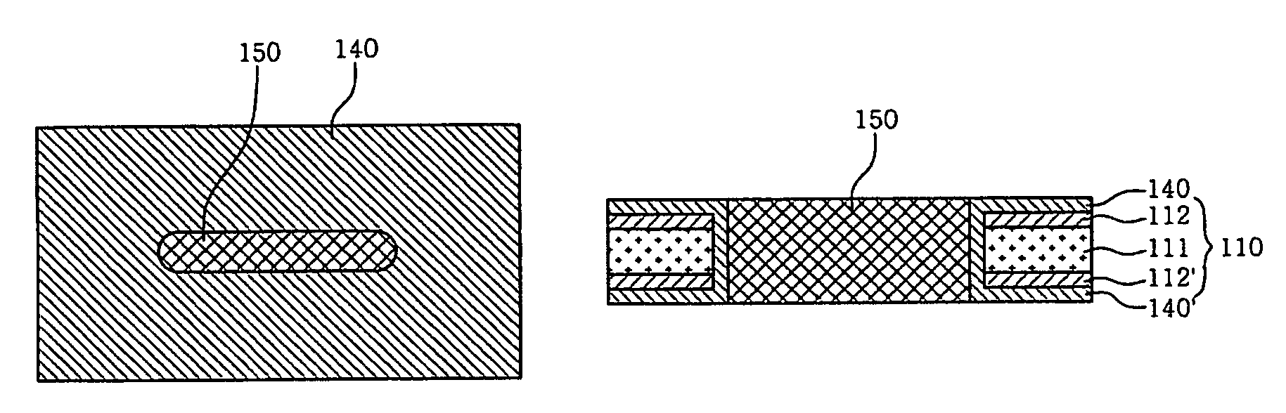
[0146]As shown in FIG. 9, in the embedded resistor according to the embodiment of the present invention, the copper-plated walls of the via holes (A3) are used as resistor terminals, the resistive material 350 is packed in an elongated hole between the via holes (A3), and it is possible to form resistors having consistent resistance values because the size and length of each elongated hole (B3) are constant.

[0147]Furthermore, the embedded resistor employing the blind via holes according to the pres...


PUM


Abstract

Disclosed is a PCB including an embedded resistor and a method of fabricating the same. The PCB includes a plurality of circuit layers in which circuit patterns are formed. A plurality of insulating layers is each interposed between the circuit layers. The embedded resistor is made of a resistive material and received in a receiving hole formed in the plurality of circuit layers and the plurality of insulating layers such that walls defining the receiving hole extends from one of the circuit layers to another circuit layer. The receiving hole has a closed section, and a conductive material is plated on the opposite walls of the walls defining the receiving hole.

Description

BACKGROUND OF THE INVENTIONINCORPORATION BY REFERENCE[0001]The present application claims priority under 35 U.S.C. §119 to Korean Patent Application No. 2004-69626 filed on Sep. 1, 2004. The content of the application is incorporated herein by reference in its entirety.[0002]1. Field of the Invention[0003]The present invention relates, in general, to a printed circuit board (PCB) including embedded resistors and a method of fabricating the same and, more particularly, to a PCB including embedded resistors, in which a resistive material is packed in a predetermined elongated hole for communicating with each other via holes, and in which walls of the via holes are used as resistor terminals, and a method of fabricating the same.[0004]2. Description of the Prior Art[0005]Recently, electronic technologies are moving toward the embedding of resistors, capacitors, integrated circuits (IC) or the like into a substrate so as to cope with demand for miniaturization and sophisticated function...

Claims


Application Information

Patent Timeline
Patent Type & Authority Patents(United States)
IPC IPC(8): H01C1/012
CPCH01C7/003H01C17/0652H05K1/167H01C17/065H01L2924/01019H01L2224/16H01L2924/01046H01L2924/01078H01L2924/01079H05K3/0047H05K3/005H05K3/4069H05K3/42H05K3/429H05K3/4652H05K2201/09509H05K2201/09645H05K2203/1476H01L2224/05001H01L2224/05023H01L2224/05568H05K1/16
Inventor KANG, MYUNG SAMRYU, CHANG SUPHONG, JONG KUK
Owner SAMSUNG ELECTRO MECHANICS CO LTD
Why Eureka
Try Eureka