Integrator-based current sensing circuit for reading memory cells

a current sensing circuit and memory cell technology, applied in the field of integrated circuits, can solve the problems of increasing the signal on the line bld, requiring a considerable amount of power, and requiring time-consuming equalization operations, and achieves the effects of large current-to-voltage transfer function, small size, and high sensitivity of the sensing circui

Inactive Publication Date: 2007-10-09
LONGITUDE LICENSING LTD
View PDF8 Cites 11 Cited by
  • Summary
  • Abstract
  • Description
  • Claims
  • Application Information

AI Technical Summary

Benefits of technology

[0010]The present invention provides several benefits over conventional cell measuring methods. First, because the source current is measured instead of the source voltage, power is saved because there is no need to charge and discharge bit lines at the source side (i.e., the source side voltage level remains close to ground). Further, the random internal voltage offset effect is avoided because each sensing circuit includes its own offset cancellation mechanism, which is directly derived from the sensing concept. In particular, each integrator is set, prior to sensing, to its DC operation level, and this level is isolated from the input and output of the integrator using the isolation and feedback capacitors. The mismatch between bit line and metal line parasitic capacitance are also solved because the integration (feedback) capacitor is an intentionally-formed element, and not a parasitic capacitor. Finally, another advantage is the sensitivity of the sensing circuit, due to the fact that integration (feedback) capacitor is a non-parasitic device, its size can be small, creating a large current-to-voltage transfer function, resulting in high accuracy and low offset.
[0011]In accordance with an embodiment of the present invention, one or more neighboring bit lines are also coupled to the sense amplifier during the read process, thus reducing or eliminating the neighbor effect by conveying any current passing through neighboring cells to the sensing circuit.

Problems solved by technology

Unfortunately, a high threshold level requires that the cell being sensed (read) be given a sufficient amount of time to fully develop its signal, thereby ensuring that, for an erased cell, the resultant signal has reached its full (high) voltage level.
However, this equalization operation is time-consuming and requires a considerable amount of power.
A problem with the approach taught by Dr.
Therefore, the amount of leakage is difficult to predict and compensate for because the amount of leakage is at least partially dependent on the programmed state of neighbor cell 10N, neighbor's neighbor cell 10N2, and so on.
In the worst case, if the sensed cell is only partially erased and the neighbor cells 10N and 10N2 are erased, the resulting current drawn through these neighbor cells can cause the signal on line BLD to increase more slowly than if the sensed cell were programmed, thereby possibly resulting in an erroneous “cell programmed” (logic 0) detection when cell 10A is in fact erased.
In addition to the neighbor effect, another problem encountered by the approach taught by Dr.
Eitan is that comparator 22 is subject to random internal voltage offsets that can also cause erroneous programmed / erased readings.
Random internal voltage offsets arise in these multiple comparators for various reasons, including device geometry mismatches and process fluctuations.
Because these internal voltage offsets are random, and because the near-ground voltage signals read by the comparators leave very little room for error, two comparators 22 may generate different programmed / erased readings for the same sensed cell signal VCELL and reference signal VREF, thus resulting in erroneous programmed / erased readings.
Another cause of voltage offsets is the parasitic capacitance of bit lines and decoding lines, which are charged while sensing and directly relate to the sensing accuracy.
A mismatch between the reference capacitance and any cell capacitance may cause offset.

Method used


Image

  • Integrator-based current sensing circuit for reading memory cells
  • Integrator-based current sensing circuit for reading memory cells
  • Integrator-based current sensing circuit for reading memory cells

Examples


Embodiment Construction

[0027]The present invention is directed to the operation of non-volatile memory (NVM) cells using near-ground signals in a manner that prevents the erroneous neighbor effect described above. While the invention is described herein with specific reference to simplified NVM cells arranged in a simplified NVM array, it is noted that the present invention may be applied to many types of NVM cells (e.g., EPROM, EEPROM, flash, one-time programmable (fuse) cells, and multi-bit NVM cells such as those disclosed in U.S. Pat. No. 6,011,725, which is incorporated herein by reference) be utilized in many circuit settings (e.g., as dedicated NVM devices, or part of a more complex integrated circuit). Accordingly, the memory circuits described below are intended to be illustrative and not limiting.

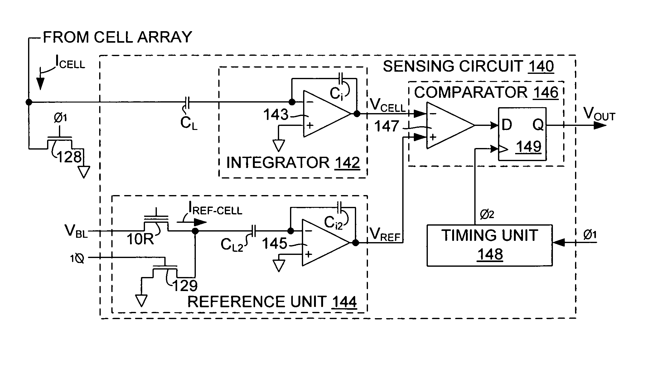
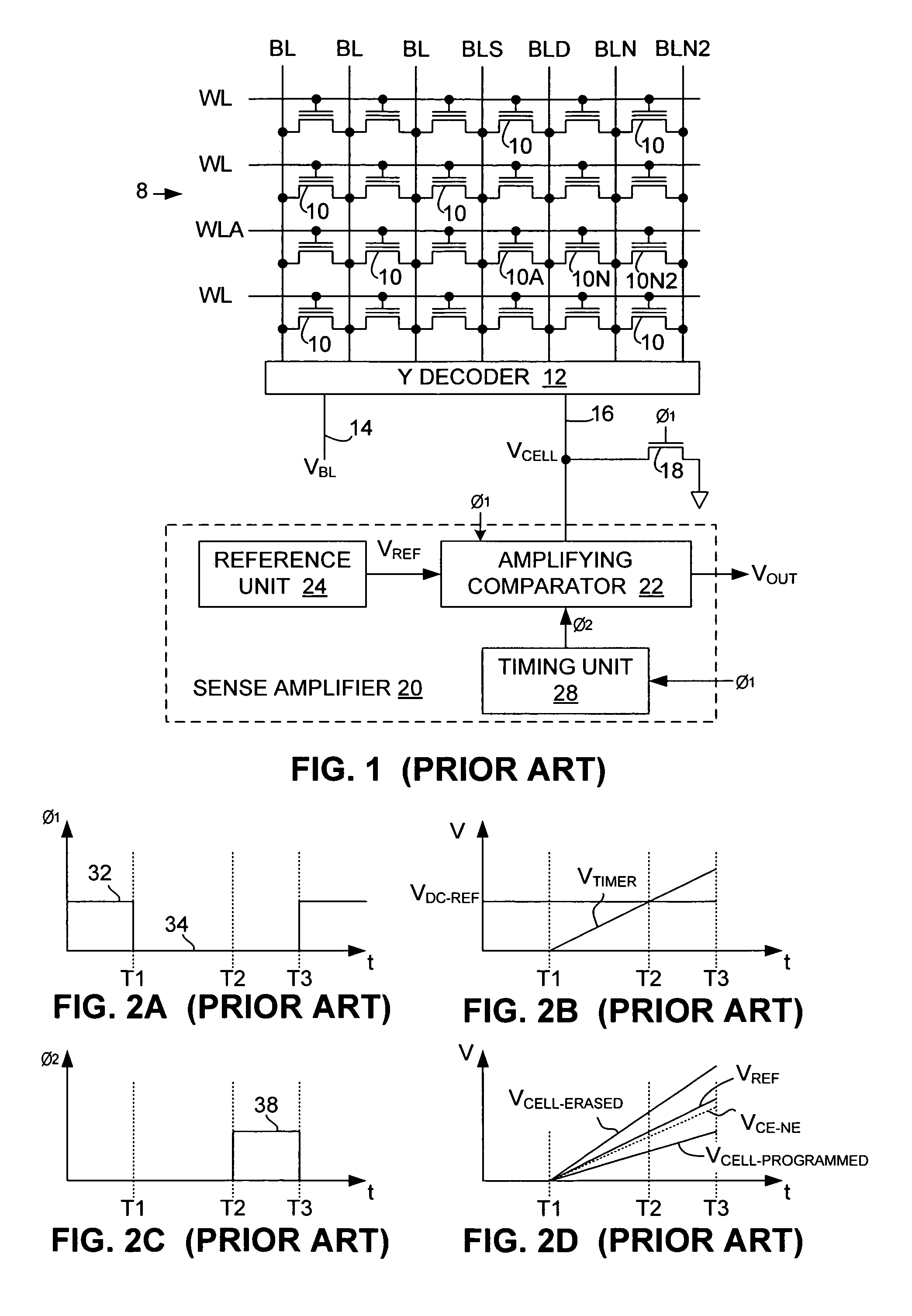
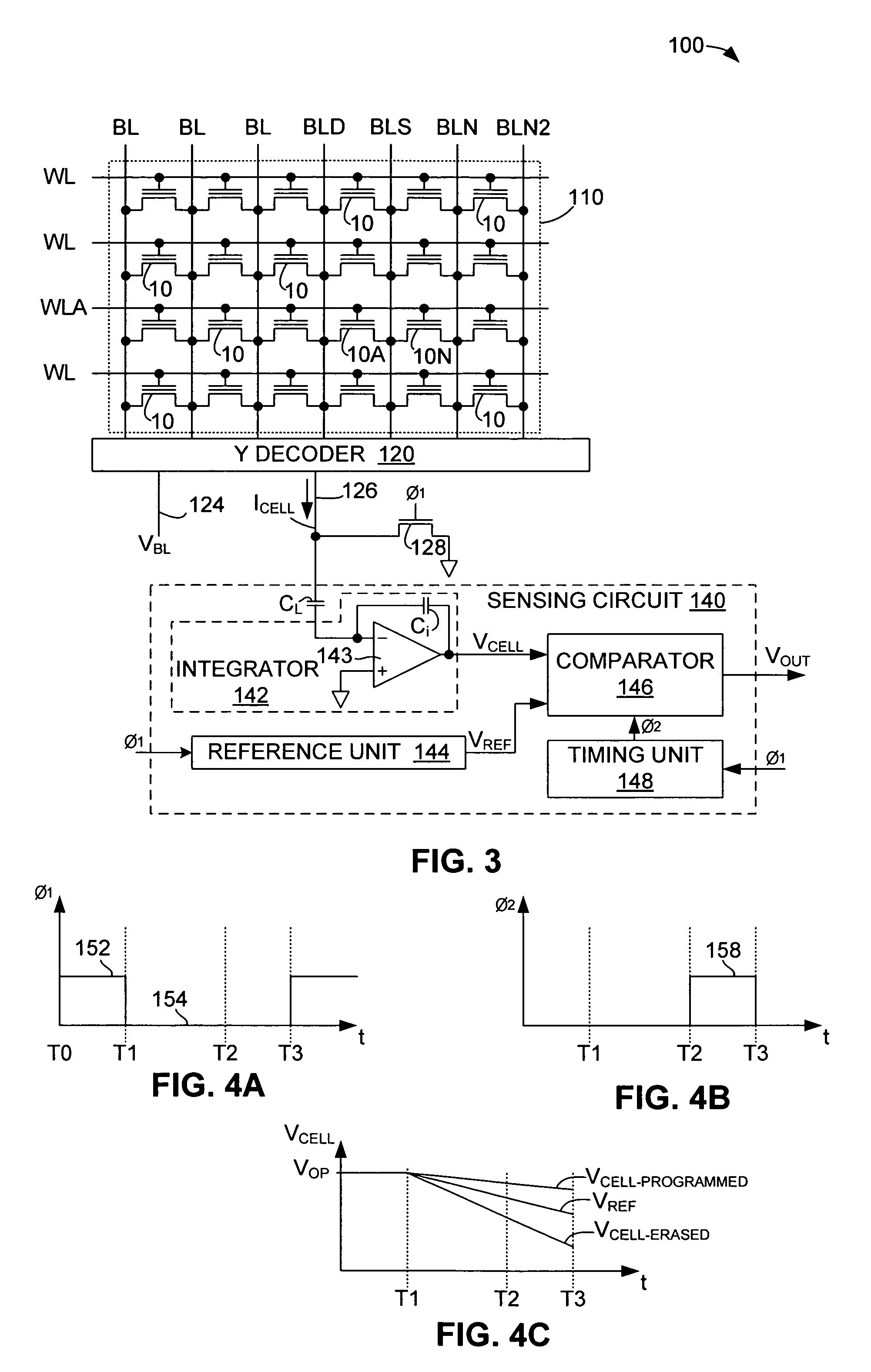
[0028]FIG. 3 shows a memory circuit 100 including an array 110 and a Y decoder (e.g., a multiplexer) 120 that operate in a manner similar to that disclosed in U.S. Pat. No. 6,128,226 (discussed above an...


PUM


Abstract

Near-ground sensing of non-volatile memory (NVM) cells is performed on a selected NVM cell by applying a potential to a first terminal, coupling a second terminal to ground, and then decoupling the second terminal and passing the resulting cell current to an integrator, which generates a corresponding sense voltage. The amount of cell current (and resulting sense voltage) is controlled by the programmed / erased state of the NVM cell. The sense voltage is compared with a reference voltage to determine the cell's programmed / erased state. Current through neighbor cells is redirected to the sensing circuit using a special Y decoder to minimize the neighbor effect.

Description

RELATED APPLICATION[0001]The present application claims priority of U.S. Patent Application Ser. No. 60 / 635,851 filed by Erez Sarig on Dec. 14, 2004.FIELD OF THE INVENTION[0002]The present invention relates to integrated circuit (IC) devices that operate using close to ground level (“near-ground”) voltage signals. More specifically, the present invention relates to methods and architectures for sensing the programmed state of memory cells using near-ground signals.RELATED ART[0003]Memory devices, such as random access memory (RAM), read-only memory (ROM), non-volatile memory (NVM) and like, are known in the art. These devices provide an indication of the data that is stored therein by providing an output electrical signal. In general, conventional sense amplifiers determine the logical value stored in a cell by comparing, after a suitable set-up period, this output electrical signal with a fixed threshold voltage level. If the output signal is above the threshold, the cell is determ...

Claims


Application Information

Patent Timeline
Patent Type & Authority Patents(United States)
IPC IPC(8): G11C16/06
CPCG11C16/28G11C16/0491
Inventor SARIG, EREZ
Owner LONGITUDE LICENSING LTD
Why Eureka
Try Eureka