Coating and developing system and coating and developing method

a technology of coating and developing system, applied in the direction of printers, instruments, photosensitive materials, etc., can solve the problems of contaminated carrying arms, coating and developing system contaminated entirely with particles, contaminated carrying arms, etc., to achieve accurate resist pattern, prevent obstruction of the developing process by water marks, and accurate resist pattern

Active Publication Date: 2007-10-23
TOKYO ELECTRON LTD
View PDF3 Cites 4 Cited by
  • Summary
  • Abstract
  • Description
  • Claims
  • Application Information

AI Technical Summary

Benefits of technology

[0011]The present invention has been made to solve those problems and it is therefore an object of the present invention to provide a coating developing system and a coating and developing method capable of restraining particle contamination when a resist film is formed on a substrate by applying a resist to the substrate and the resist film processed by immersion exposure is developed. Another object of the present invention is to provide a coating and developing system and a coating and developing method capable of preventing processing a substrate by an abnormal developing process due to water marks formed on the substrate when a liquid used for immersion exposure dries.
[0019]According to the present invention, the first carrying mechanism carries the substrate processed by immersion exposure by the exposure system to the substrate cleaning unit, and then the substrate cleaning unit cleans the substrate. Therefore, even if the substrate contaminated with particles of the resist dissolved in the liquid layer in the immersion exposure, the particles can be removed from the substrate. Since the cleaned substrate is carried by the second carrying mechanism instead of by the first carrying mechanism, the contamination of the processing units of the processing block and the substrate processed by the processing units with particles can be avoided. Consequently, adverse influences of particles on the line-width of a pattern during a heating process, damaging the pattern with particles in the developing process and obstruction of exposure by the migration of particles in the liquid layer during immersion exposure can be prevented. Thus an accurate resist pattern can be formed on a substrate.
[0020]Since the humidifying unit controls the humidity of an atmosphere through which the substrate processed by immersion exposure is carried to the substrate cleaning unit, formation of water marks due to the drying of the liquid remaining on the substrate processed by immersion exposure and being carried to the substrate cleaning unit can be prevented. Consequently, obstruction of the developing process by water marks can be restrained and an accurate resist pattern can be formed on the substrate.

Problems solved by technology

When the wafer contaminated with particles is transferred from the exposure system to the carrying arm of the interface block, the carrying arm will be contaminated with the particles.
Then, other wafers carried by the contaminated carrying arm will be contaminated with the particles.
Consequently, it is likely that the coating and developing system is contaminated entirely with particles.
Moreover, particles adhering to the wafer are likely to damage the resist pattern during the developing process.
If contamination with particles (hereinafter, referred to as “particle contamination”) spreads in the coating and developing system and a heating unit is used for processing a wafer both before and after the exposure process, a wafer to be transferred through the heating unit to the exposure system will be contaminated.
When the exposure system carries out an immersion exposure process, particles migrating in a liquid layer in an exposed area obstruct normal exposure.
Consequently, an accurate resist pattern cannot be formed and defects in the resist pattern are likely to be distributed on the wafer.
Formation of water marks is another problem other than that of particle contamination in immersion exposure.
Water marks will obstruct the normal processing of a wafer by an exposure process.

Method used


Image

  • Coating and developing system and coating and developing method
  • Coating and developing system and coating and developing method
  • Coating and developing system and coating and developing method

Examples


Embodiment Construction

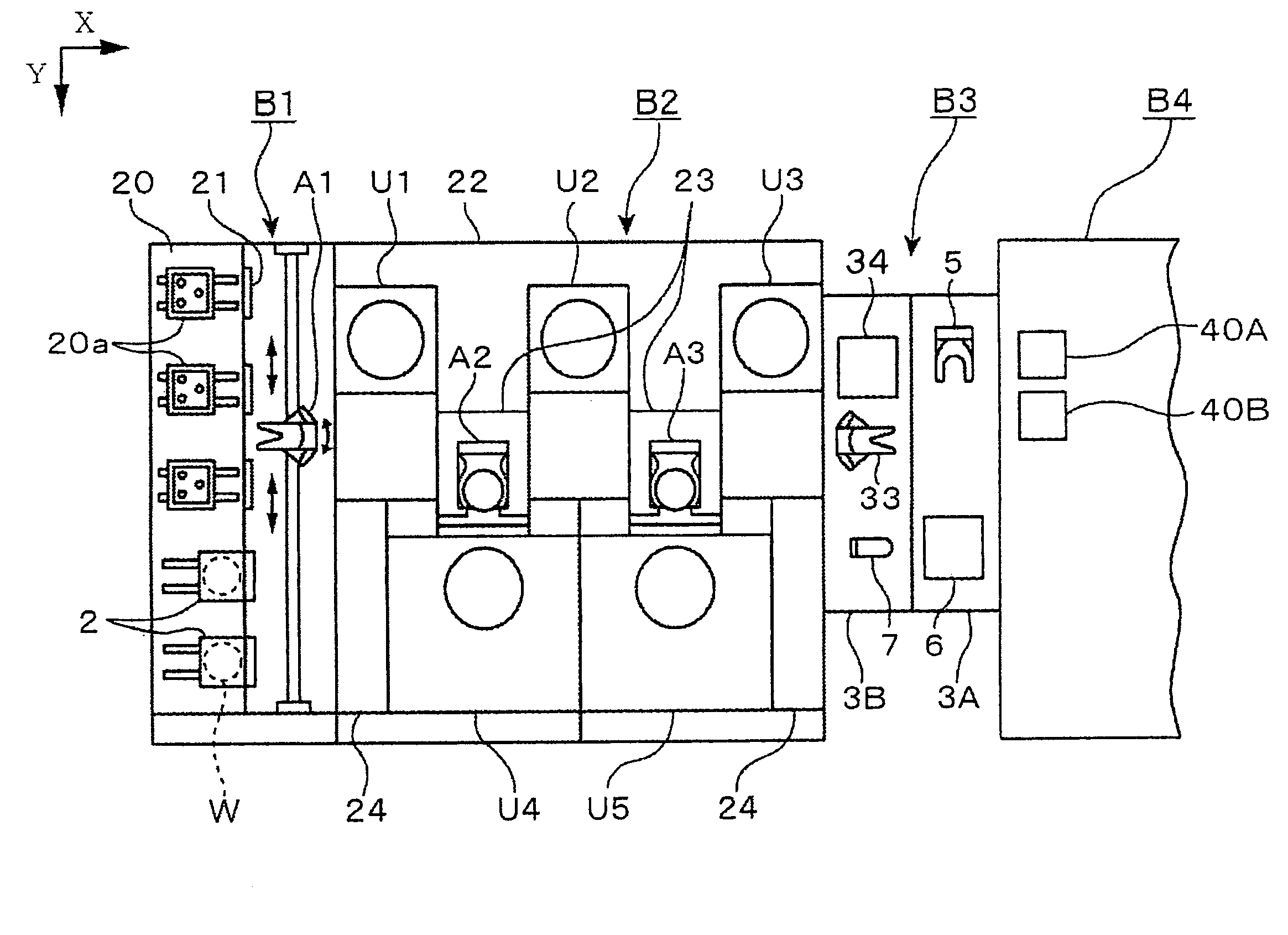
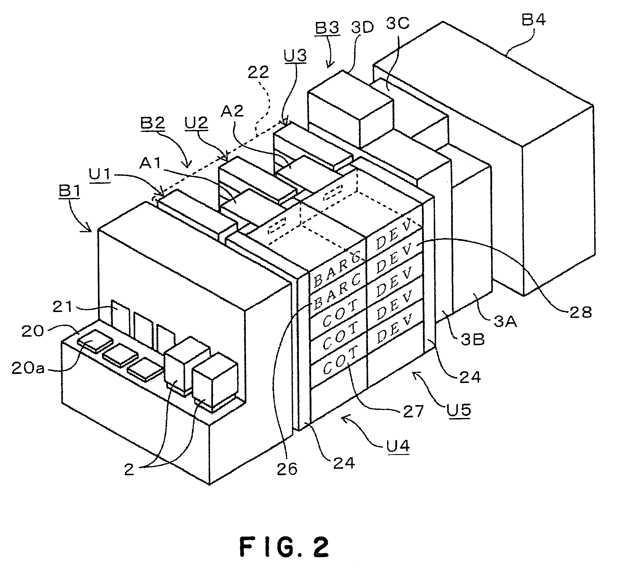
[0030]The constitution of a coating and developing system in a first embodiment according to the present invention will be described with reference to FIGS. 1 and 2. FIG. 1 is a plan view of a resist pattern forming apparatus built by connecting the coating and developing system in the first embodiment to the exposure system that carries out immersion exposure, and FIG. 2 is a perspective view of the resist pattern forming apparatus shown in FIG. 1. A carrier 2 containing, for example, thirteen wafers W is delivered to a carrier handling block B1. The carrier handling block B1 has a carrier station 20 provided with carrier support tables 20a capable of supporting a plurality of carriers 2 thereon, respectively, gates 12 formed in a wall behind the carrier support table 20a, and a transfer device A1 capable of extending through the gate 21 to the carrier 2 to take out the wafer W from the carrier 2.

[0031]A processing block B2 surrounded by a casing 22 is connected to the back end of ...


PUM


Abstract

A coating and developing system is capable of preventing the contamination of a substrate with particles while the same coats a surface of a substrate with a resist film and develops the resist film after the substrate has been processed by immersion exposure. The coating and developing system includes: a processing block including coating units for forming a resist film on a surface of a substrate and developing units for processing the resist film formed on the substrate with a developer, and an interface block connected to the processing block and an exposure system for carrying out an immersion exposure process. The interface block includes: substrate cleaning units for cleaning the substrate processed by the immersion exposure process, a first carrying mechanism and a second carrying mechanism. The first carrying mechanism carries a substrate processed by immersion exposure to the substrate cleaning unit. The second carrying mechanism carries the substrate cleaned by the substrate cleaning unit. Thus the contamination of the substrate with external particles can be prevented and hence the spread of contamination with particles over the processing units of the processing block and substrates processed by the processing units can be prevented.

Description

BACKGROUND OF THE INVENTION[0001]1. Field of the Invention[0002]The present invention relates to a coating and developing system including a coating unit for coating a surface of a semiconductor wafer (hereinafter, referred to simply as “wafers”) with a resist film and a developing unit for developing the resist film processed by immersion exposure by using a developer, and a coating and developing method.[0003]2. Description of the Related Art[0004]A photoresist pattern forming process, namely, one of semiconductor device fabricating processes, includes the steps of forming a resist film on a surface of a wafer by applying a resist to the surface of the wafer, exposing the resist film in a predetermined pattern, and developing the exposed resist film by using a developer to form a resist pattern. Generally, this photoresist pattern forming process is carried out by a system built by connecting an exposure system to a coating and developing system including a coating unit and a deve...

Claims


Application Information

Patent Timeline
Patent Type & Authority Patents(United States)
IPC IPC(8): G03D5/00G03B27/32G03B27/52
CPCH01L21/67178H01L21/67745H01L21/67184H01L21/67051Y10S134/902H01L21/67742E06B3/6604E06B3/66376
Inventor ISHIDA, SEIKINAKAHARADA, MASAHIROYAMAMOTO, TARO
Owner TOKYO ELECTRON LTD
Why Eureka
Try Eureka