
Semiconductor package and method for manufacturing the same

a technology of semiconductor and packaging, applied in the direction of semiconductor/solid-state device details, semiconductor devices, electrical apparatus, etc., can solve the problems of not fully meeting the requirements of semiconductor packaging, the manufacturing method in the prior art still has many limitations, and the operation speed and complexity of ic chips have become higher and higher, so as to reduce the packaging cost and improve the packaging reliability

Active Publication Date: 2007-10-23
ADVANCED SEMICON ENG INC
View PDF10 Cites 30 Cited by
  • Summary
  • Abstract
  • Description
  • Claims
  • Application Information

AI Technical Summary

Benefits of technology

The present invention provides a semiconductor package and a method for manufacturing it that offers higher packaging efficiency and eliminates limitations and drawbacks in the prior art. The semiconductor package comprises a chip, pad extension traces, via holes, a lid, and metal traces. The chip has an active surface, a back surface, an optical component, and bonding pads connected to the optical component. The pad extension traces are connected to the bonding pads. The via holes are formed through the chip and connected to the pad extension traces. The lid is attached on the chip's active surface. The metal traces are on the chip's back surface and connected to the via holes. The metal traces define solder pads. This semiconductor package can be mass-produced at wafer level, reducing packaging cost and improving reliability.

Problems solved by technology

Further, as the demands for lighter and more complex electronic devices gradually increase, the operating speed and the complexity of IC chips have become higher and higher.
However, theses semiconductor packages and the manufacturing methods in the prior art still have many limitations and drawbacks, and therefore can not completely meet the requirements for semiconductor packages.

Method used


Image

  • Semiconductor package and method for manufacturing the same
  • Semiconductor package and method for manufacturing the same
  • Semiconductor package and method for manufacturing the same

Examples


first embodiment

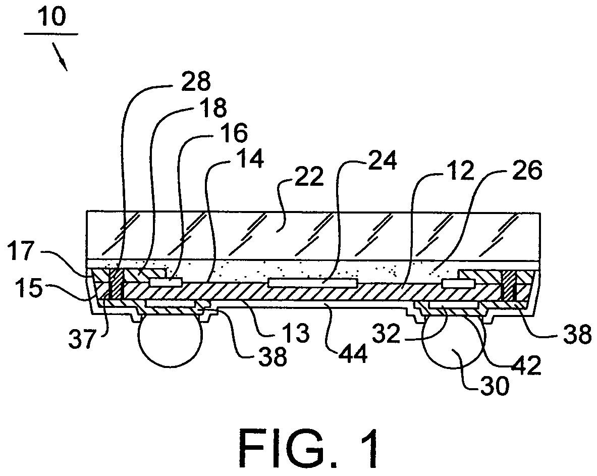
[0026]Now referring to FIG. 1, it shows a sectional view of a semiconductor package 10 of the present invention. The semiconductor package 10 comprises a chip 12 having an active surface 14, a back surface 13 opposite to the active surface, an optical component 24 (e.g. sensor and photo coupler) disposed on the active surface 14, and a plurality of bonding pads 16 disposed on the active surface 14. The optical component 24 can be formed by complementary metal oxide semiconductor (CMOS).

[0027]The chip 12 further has a plurality of via holes 28 formed through the chip 12 and a plurality of pad extension traces 18 for electrically connecting the bonding pads 16 to the via holes 28. The semiconductor package 10 further comprises a lid 22 being attached on the active surface 14 of the chip 12 through an adhesive layer 26, and covering the active surface 14 and the plurality of pad extension traces 18.

[0028]The semiconductor package 10 further comprises a plurality of compliant pads 32, ...

second embodiment

[0046]Now referring to FIG. 17, it shows a sectional view of a semiconductor package 110 of the present invention. The semiconductor package 110 is substantially identical to the semiconductor package 10, and its similar elements will be indicated by the same numerals. The solder mask 144 of the semiconductor package 110 is only coated on the back surface 13 of the chip 112 and not coated on the side surfaces 115 of the same. Further, the chip 112 has vertical side surfaces 115 instead of the inclined side surfaces.

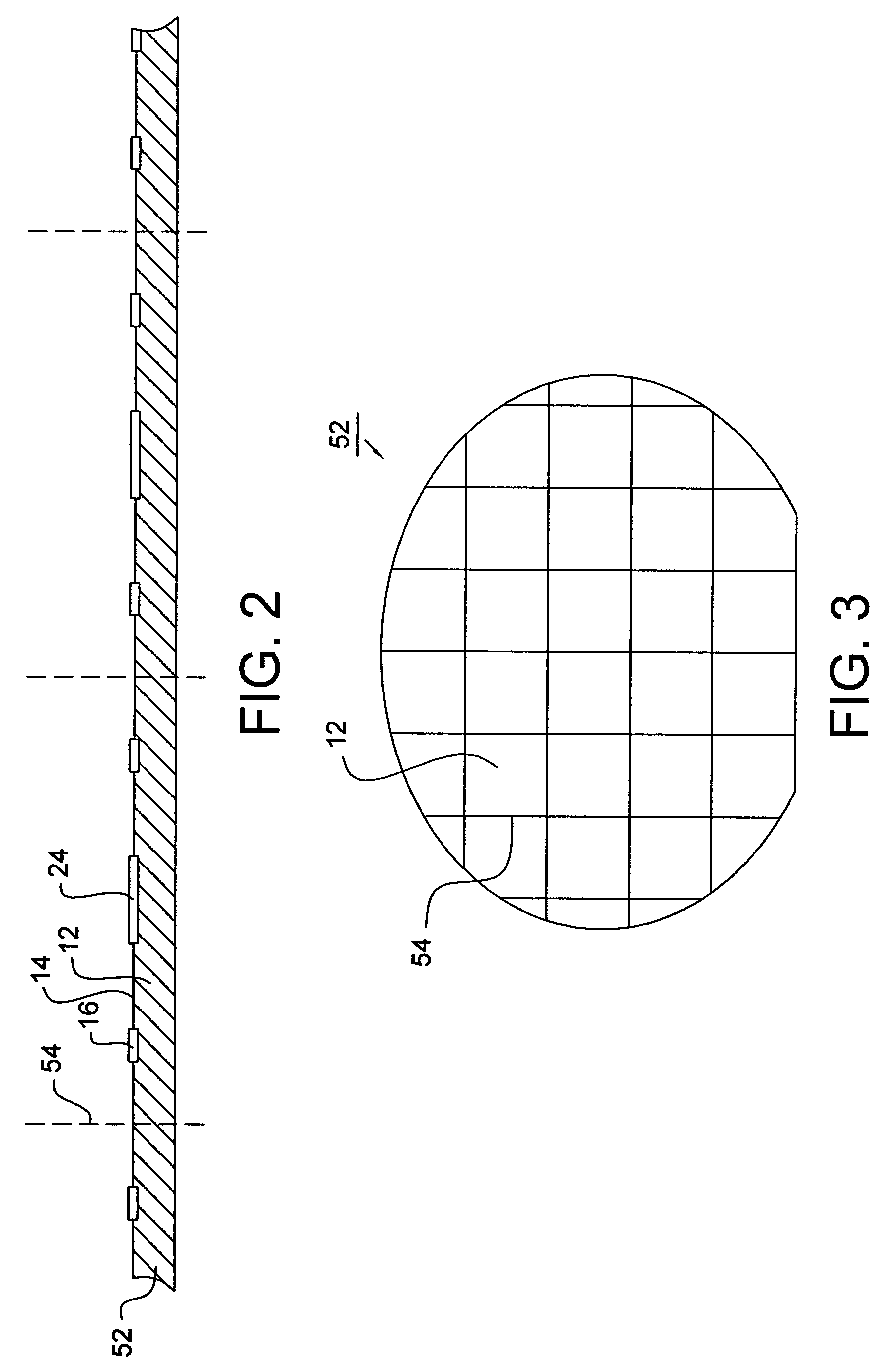
[0047]Now referring to FIGS. 2 to 12 and FIGS. 18 to 20, they illustrate a method for manufacturing the semiconductor package 110 according to present invention.

[0048]Referring to FIG. 18, a solder mask 144 is coated on the back surface 13 of the wafer 52 with parts of the metal traces 38 exposed therefrom, such that the parts can be defined as a plurality of solder pads 42.

[0049]Referring to FIG. 19, a plurality of solder balls 30 are respectively disposed on the solder...

third embodiment

[0052]Now referring to FIG. 22, it shows a sectional view of a semiconductor package 210 of the present invention. The semiconductor package 210 is substantially identical to the semiconductor package 110, and its similar elements will be indicated by the same numerals. In this embodiment, the via holes 28a are exposed out of the side surfaces 210a of the semiconductor package 210.

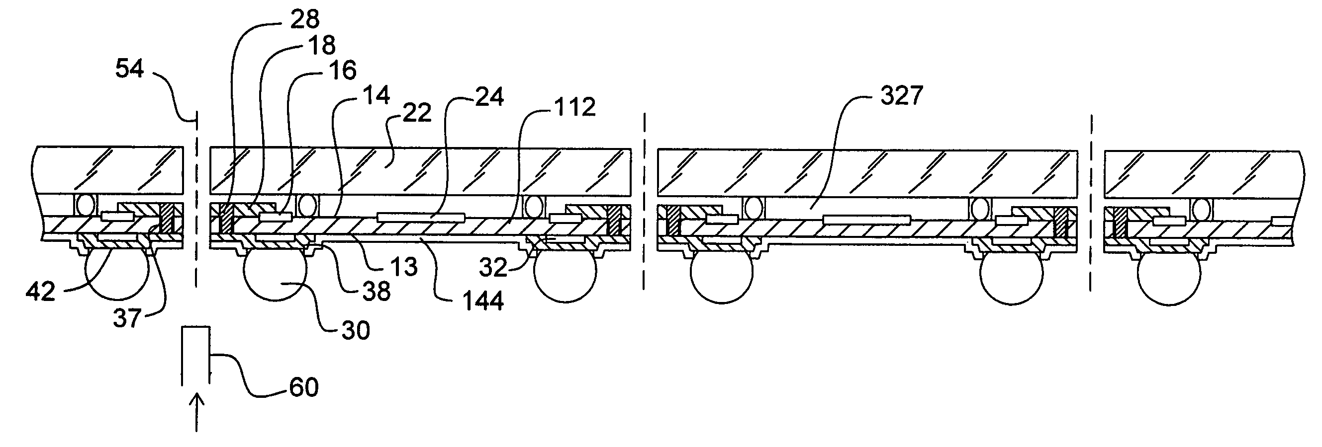
[0053]Now referring to FIGS. 2 to 5 and FIGS. 23 to 32, they illustrate a method for manufacturing the semiconductor package 210 according to present invention.

[0054]Referring to FIG. 23, a plurality of holes 36 are formed through the pad extension traces 18 on the scribe lines 54 by using a laser drill 40 and each hole 36 has a predetermined depth.

[0055]Referring to FIG. 24, the photoresist 20 is striped off and an insulating layer 37 is formed on the inner surface of each hole 36 according to the same manner illustrated in FIG. 7.

[0056]Referring to FIG. 25, a plurality of via holes 28 are formed and ele...


PUM


Abstract

A semiconductor package comprises a chip, a plurality of pad extension traces, a plurality of via holes, a lid and a plurality of metal traces, wherein the chip has an active surface, a back surface opposite to the active surface, an optical component disposed on the active surface, and a plurality of pads disposed on the active surface and electrically connected to the optical component; the pad extension traces are electrically connected to the pads; the via holes are formed through the chip and electrically connected to the pad extension traces; the lid is attached on the active surface of the chip; and the plurality of metal traces are disposed on the back surface of the chip, electrically connected to the plurality of via holes, and defines a plurality of solder pads thereon.

Description

BACKGROUND OF THE INVENTION [0001]1. Field of the Invention[0002]This invention generally relates to a semiconductor package and a method for manufacturing the same, and more particularly to a wafer level semiconductor package and a method for manufacturing the same.[0003]2. Description of the Related Art[0004]The semiconductor package provides four functions, i.e. signal distribution, power distribution, heat dissipation and element protection. In general, a semiconductor chip is packaged into an enclosure (e.g. a single-chip module), and then disposed on a printed circuit board, together with other components, such as capacitors, resistors, inductors, filters, switches, and optical and RF components.[0005]The complementary metal oxide semiconductor (CMOS) technology for making optical components is similar to that for making semiconductor chips. CMOS is typically formed by silicon (Si) and germanium (Ge) and generally includes NMOS (negative polarity) and PMOS (positive polarity) ...

Claims


Application Information

Patent Timeline
Patent Type & Authority Patents(United States)
IPC IPC(8): H01L33/00H01L31/0224
CPCH01L23/10H01L23/3114H01L24/13H01L23/481H01L24/10H01L2224/13099H01L2924/01029H01L2924/01032H01L2924/14H01L2924/19041H01L2924/19042H01L2924/19043H01L2924/01033H01L2924/014H01L2924/00H01L2924/351H01L2224/13H01L2224/05568H01L2224/05023H01L2224/05001H01L2224/056H01L2924/00014H01L2224/02372H01L2224/02313H01L24/03H01L24/05H01L2224/05548H01L2224/02123H01L2224/0215H01L2224/0236H01L31/0203H01L2224/02377H01L2224/05099H01L2924/06
Inventor YEE, KUO CHUNGLEE, CHUN CHI
Owner ADVANCED SEMICON ENG INC
Learn More