Mask, method for manufacturing a mask, method for manufacturing an electro-optical device, and electronic equipment

a manufacturing method and electro-optical technology, applied in the field of masks, can solve the problems of difficult to manufacture a large and thin metal mask with a high degree of accuracy, easy to break the mask, and inability to use the evaporation mask

Inactive Publication Date: 2007-10-23
SEIKO EPSON CORP
View PDF24 Cites 4 Cited by
  • Summary
  • Abstract
  • Description
  • Claims
  • Application Information

AI Technical Summary

Benefits of technology

[0015]According to this aspect of the present invention, since the mask includes a silicon part, the thermal expansion coefficient of the mask is equal or close to that of a member on which a film is deposited, that is, a glass substrate, for example. Therefore, dimensional variations in a film pattern caused by a thermal expansion difference can be reduced. According to this aspect of the present invention, since the mask includes a silicon part, the accuracy of processing the opening can be easily increased.
[0045]According to this aspect of the present invention, for example, it is possible to economically provide electronic equipment that displays bright large images without unevenness with a widescreen. Also according to this aspect of the present invention, it is possible to economically provide electronic equipment that includes an electronic circuit etc. composed of a thin film that is highly precisely patterned entirely on a large substrate.

Problems solved by technology

It is, however, difficult to manufacture a large and thin metal mask with a high degree of accuracy.
The problem is that stress tends to be concentrated in the corners of the evaporation mask described in Japanese Unexamined Patent Publication No. 2001-185350, and the mask is easily broken once a force is applied to it.
Therefore, it is impractical to use the evaporation mask using the silicon substrate described in Japanese Unexamined Patent Publication No. 2001-185350 in equipment manufacturing sites.
Meanwhile, it becomes difficult to form a thin film pattern with sufficient dimensional accuracy as the radius of the rounded corner is larger than 3.0 μm.
Therefore, this method can easily provide a mask for forming a thin film pattern with a high degree of accuracy and whose corners are hard to break and endure repetitive use.

Method used


Image

  • Mask, method for manufacturing a mask, method for manufacturing an electro-optical device, and electronic equipment
  • Mask, method for manufacturing a mask, method for manufacturing an electro-optical device, and electronic equipment
  • Mask, method for manufacturing a mask, method for manufacturing an electro-optical device, and electronic equipment

Examples


Embodiment Construction

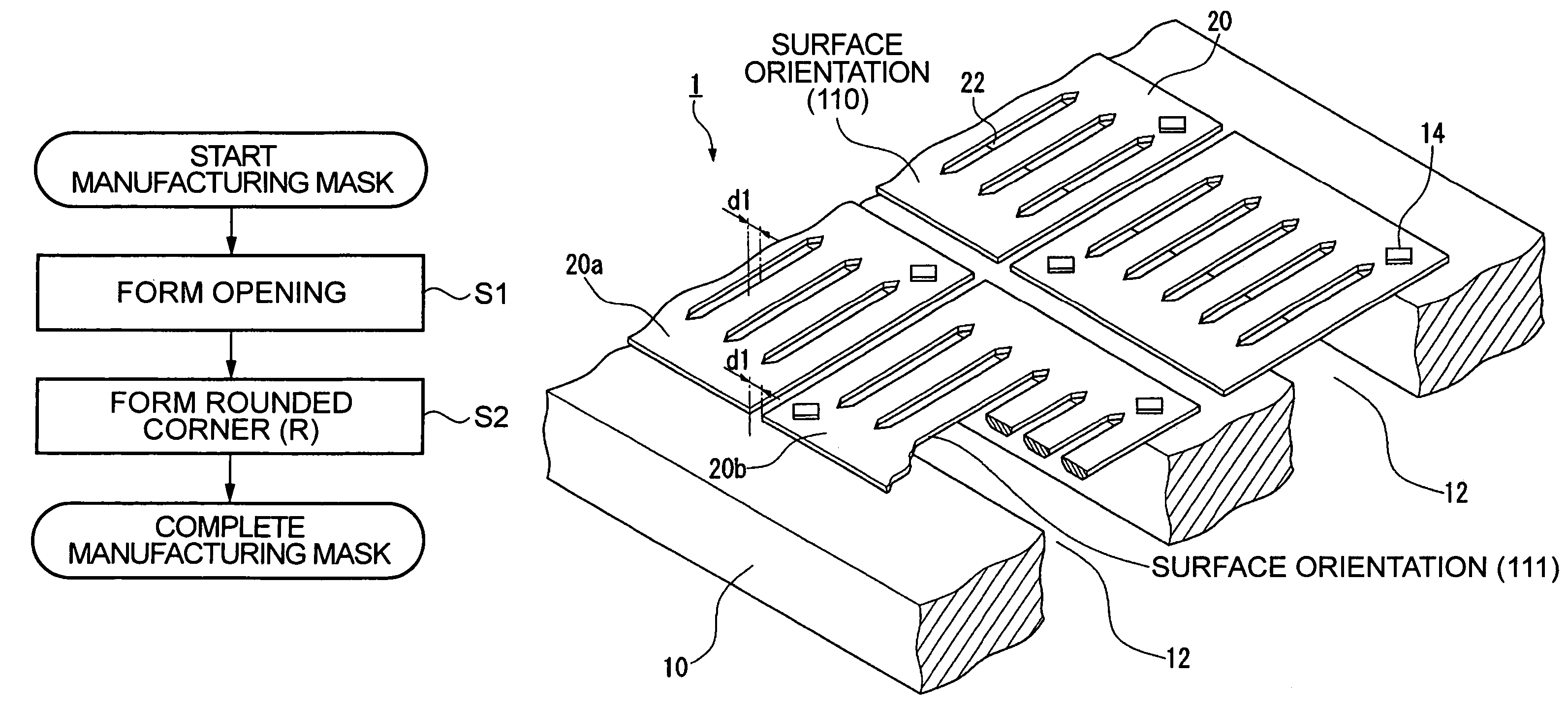
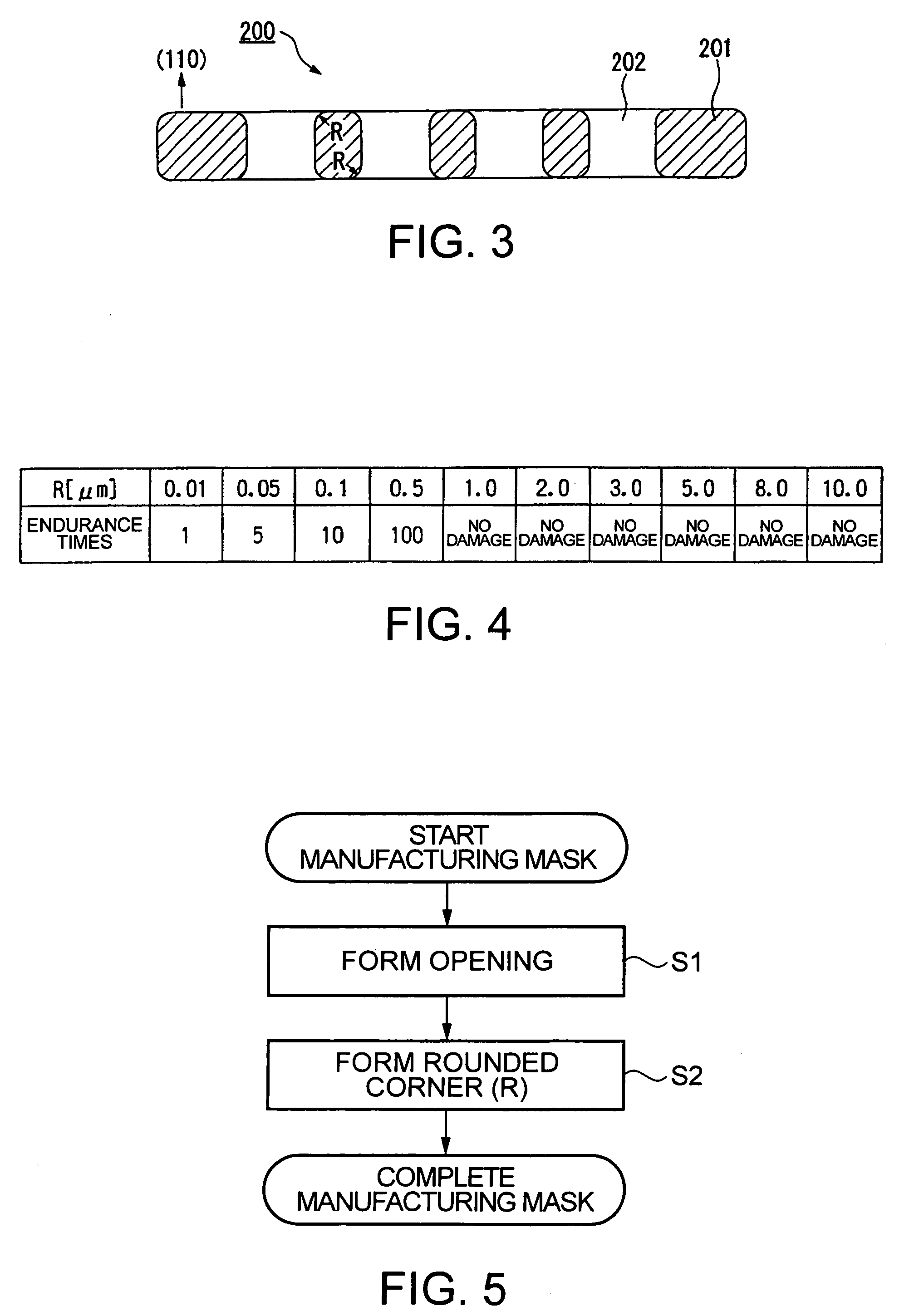
[0062]Embodiments of a mask according to the present invention will be described with reference to the accompanying drawings.

[0063]Mask Structure

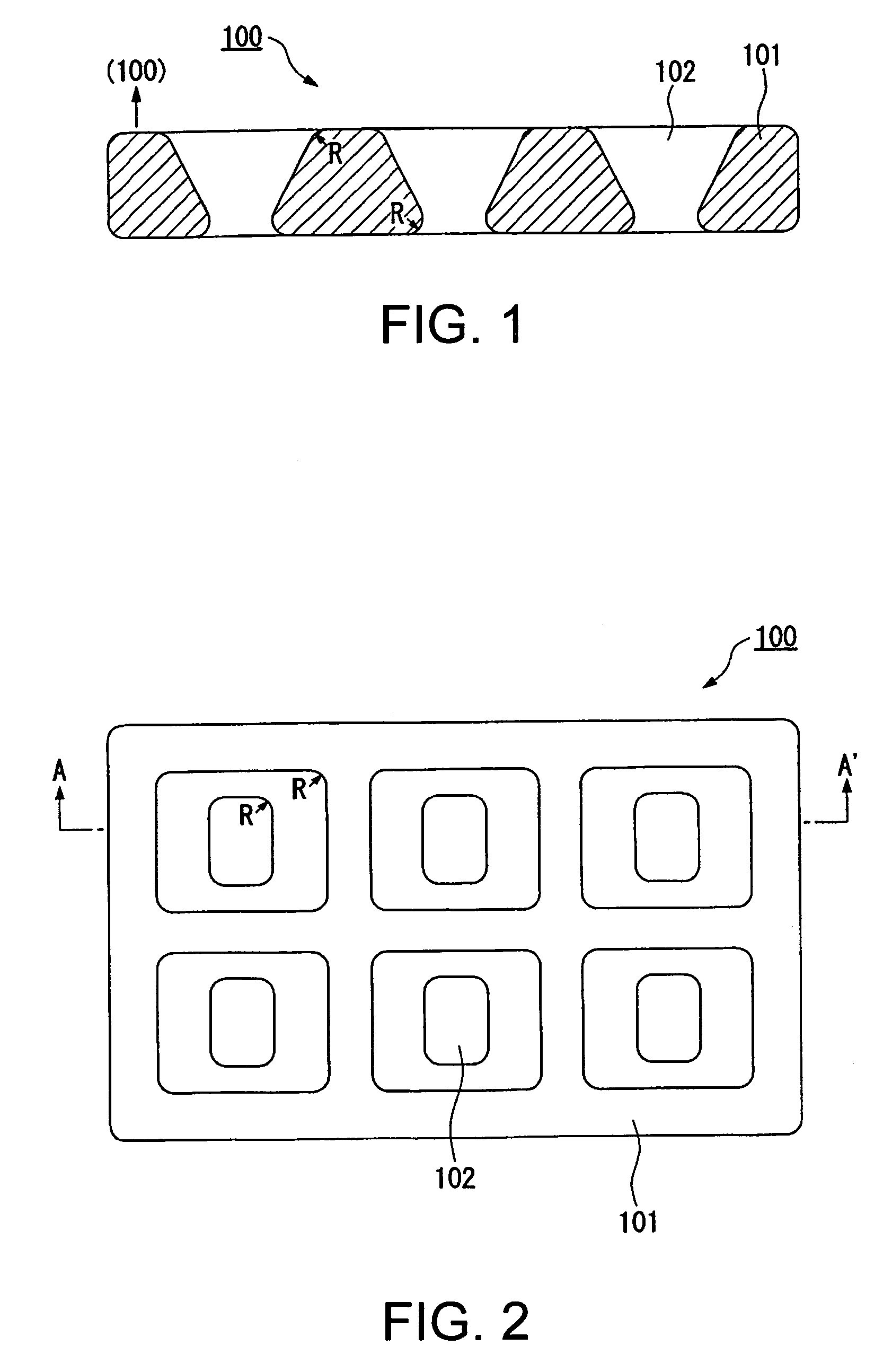
[0064]FIG. 1 is a sectional view illustrating an example of an embodiment of a mask according to the present invention. FIG. 2 is a plan view of the mask shown in FIG. 1. More specifically, FIG. 1 is a sectional view of a mask 100 along line A-A′ shown in FIG. 2. The mask 100 of the present embodiment can be used as, for example, an evaporation mask. When using the mask 100 for patterning a thin film on a member on which the film is deposited, the mask 100 is disposed between an evaporation source and the member.

[0065]The mask 100 of the present embodiment includes a silicon substrate 101. The silicon substrate 101, for example, has surface orientation (100). The silicon substrate 101 is provided with an opening 102 that forms a through-hole. The opening 102 forms a through-hole through which a material to be evaporated from the evaporation...


PUM

PropertyMeasurementUnit
radiusaaaaaaaaaa
radiusaaaaaaaaaa
radiusaaaaaaaaaa

Abstract

A mask includes a silicon member, and a portion defining an opening penetrating the silicon member; and the corner of the opening is rounded.

Description

RELATED APPLICATIONS[0001]This application claims priority to Japanese Patent Application No. 2004-104311 filed Mar. 31, 2004 which is hereby expressly incorporated by reference herein in its entirety.BACKGROUND[0002]1. Technical Field[0003]The present invention relates to a mask, a method for manufacturing a mask, a method for manufacturing an electro-optical device, and electronic equipment.[0004]2. Related Art[0005]An organic electroluminescent (EL) panel, which is a kind of electro-optical device, is made up of light-emitting, fast-response display elements having a multilayered structure of thin films. The organic EL panel forms a lightweight display that provides high-speed motion picture response, and thus has recently drawn great attention as the display panel of a flat panel display (FPD) TV, for example. A typical method for manufacturing such an organic EL panel is described in Applied Physics Letters, Vol. 51, No. 12: 913-14, 1987. Specifically, a transparent anode made ...

Claims


Application Information

Patent Timeline
Patent Type & Authority Patents(United States)
IPC IPC(8): H01L21/311C23C14/04H01L51/50H05B33/10
CPCH05B33/10E03F5/021F16L5/08
Inventor YOTSUYA, SHINICHI
Owner SEIKO EPSON CORP
Why Eureka
Try Eureka