Versatile system for cross-lateral junction field effect transistor

a junction field effect transistor and lateral junction technology, applied in the field of semiconductor devices, can solve the problems of unaddressed performance and design problems, numerous challenges generated by the circuit manufacturing process, and certain structural and behavioral properties of the conventional jfet, and achieve high current throughput, easy to adapt to, and versatile

Active Publication Date: 2007-10-30
TEXAS INSTR INC
View PDF2 Cites 2 Cited by
  • Summary
  • Abstract
  • Description
  • Claims
  • Application Information

AI Technical Summary

Benefits of technology

[0012]The present invention provides a versatile system, comprising a number of apparatus and methods, for the design and production of high performance JFET structures. The system of the present invention provides a cross-lateral JFET architecture that is highly versatile and readily adaptable to a number of design or performance requirements. JFETs according the present invention are nonetheless capable of high-voltage, high current throughput at high frequencies. Furthermore, using the system of the present invention, JFETs are readily produced using commercially viable semiconductor process technologies. The present invention thereby provides high performance JFETs in an easy, efficient and cost-effective manner.
[0013]Specifically, the system of the present invention provides a cross-lateral JFET architecture, defined by source / drain branches orthogonal to gate branches. The gate branches of this architecture provide a well-defined gate modulation (or junction modulation) region. Parasitic capacitance effects originating from channel sidewalls are effectively eliminated. Non-linearity, otherwise associated with parasitic capacitance in conventional JFET designs, is minimized—providing optimal frequency performance. The dual gate configuration of the present invention provides dynamic pinch-off across the channel, improving the transistor gain (gm). The outer regions of each cross-lateral branch are readily accessible to implantation processes, providing for independently selective doping profiles in each such branch. Furthermore, each such branch can be customized to provide, for example, a desired contact size or shape. The system of the present invention thus provides a wide range of transistor operational voltage ranges with only minor in-process adjustments.

Problems solved by technology

The increased packing density of the integrated circuit generates numerous challenges to the semiconductor manufacturing process.
Ongoing efforts to reduce transistor geometries give rise to a number previously unaddressed performance and design issues, particularly in specialized or high-performance designs.
Unfortunately, though, conventional JFETs have certain structural and behavioral properties that limit their usefulness in high-performance applications (e.g., high frequency, high voltage).
In comparison to MOSFETs, JFETs have relatively high current capacities but relatively low gain.
This has, correspondingly, resulted in attempts to implement JFET architectures in commercial, MOS-type, photolithographic process technologies—raising a number of new issues and concerns.
This parasitic capacitance can degrade the frequency performance of the JFET.
They do, however, contribute a significant amount of additional capacitance, greatly increasing the non-linearity of the parasitic capacitance and further impairing the frequency performance of the JFET.
Where such a structure is present, the non-linear parasitic capacitance is increased even further—decreasing the JFET's frequency performance.
In most commercial applications, however, this is extremely impractical due to the cost and process overhead involved.
Thus, the presence of a backside gate typically adds nothing to the control of junction field effects while further degrading the frequency performance of the JFET.
Unfortunately, most conventional fabrication processes (e.g., lithography) are limited in their ability to reliably produce transistor features of extremely small dimension.
Aside from such production difficulties, an extremely fine channel structure would cause other performance problems—particularly with respect to frequency performance.
A gate contact to an extremely narrow channel would have extremely high resistance that would, consequently, degrade the frequency response of the transistor.
Thus, in conventional processes, the ability to limit detrimental capacitance effects through channel length reduction is of little practical value.

Method used


Image

  • Versatile system for cross-lateral junction field effect transistor
  • Versatile system for cross-lateral junction field effect transistor
  • Versatile system for cross-lateral junction field effect transistor

Examples


Embodiment Construction

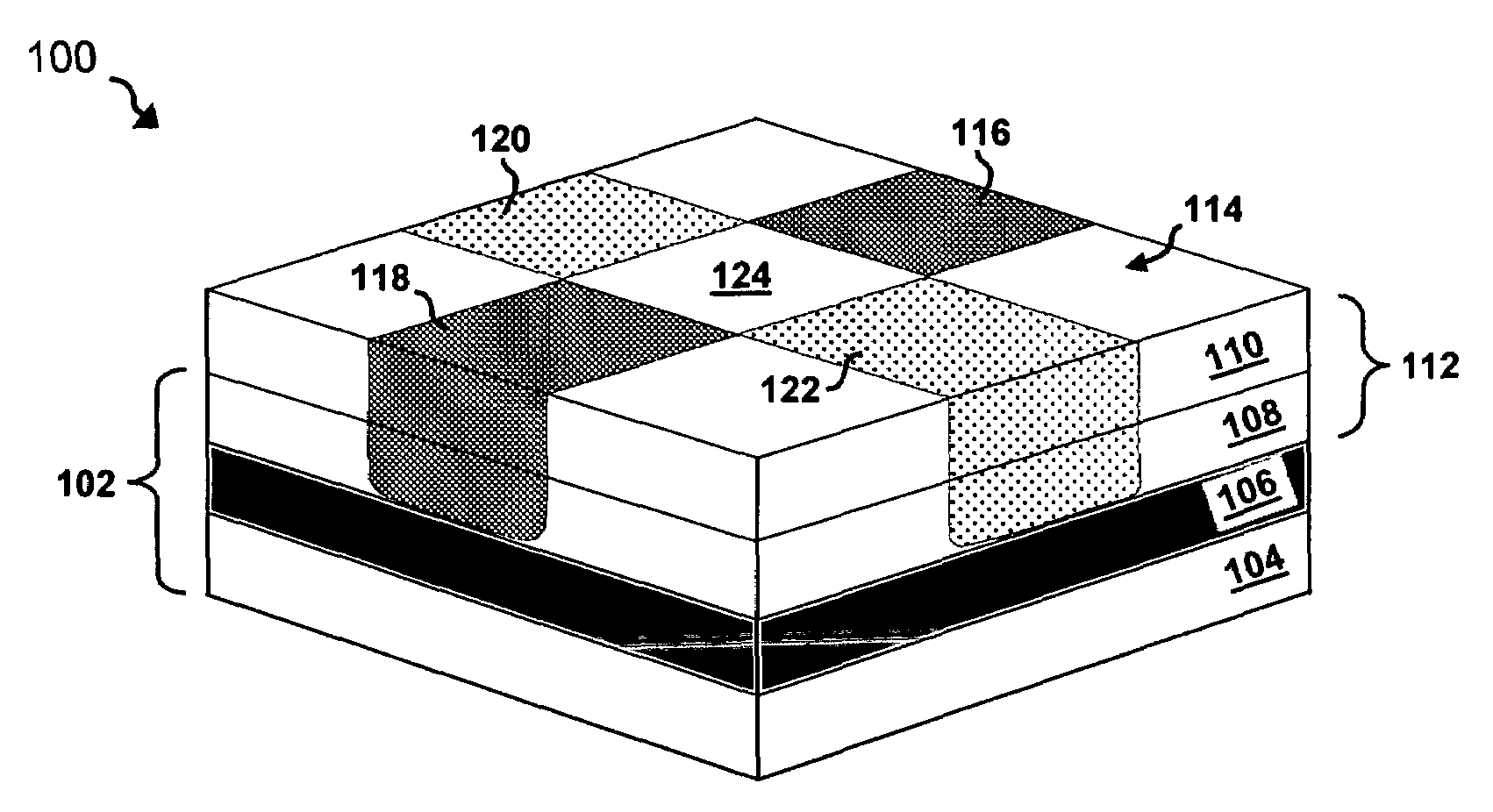
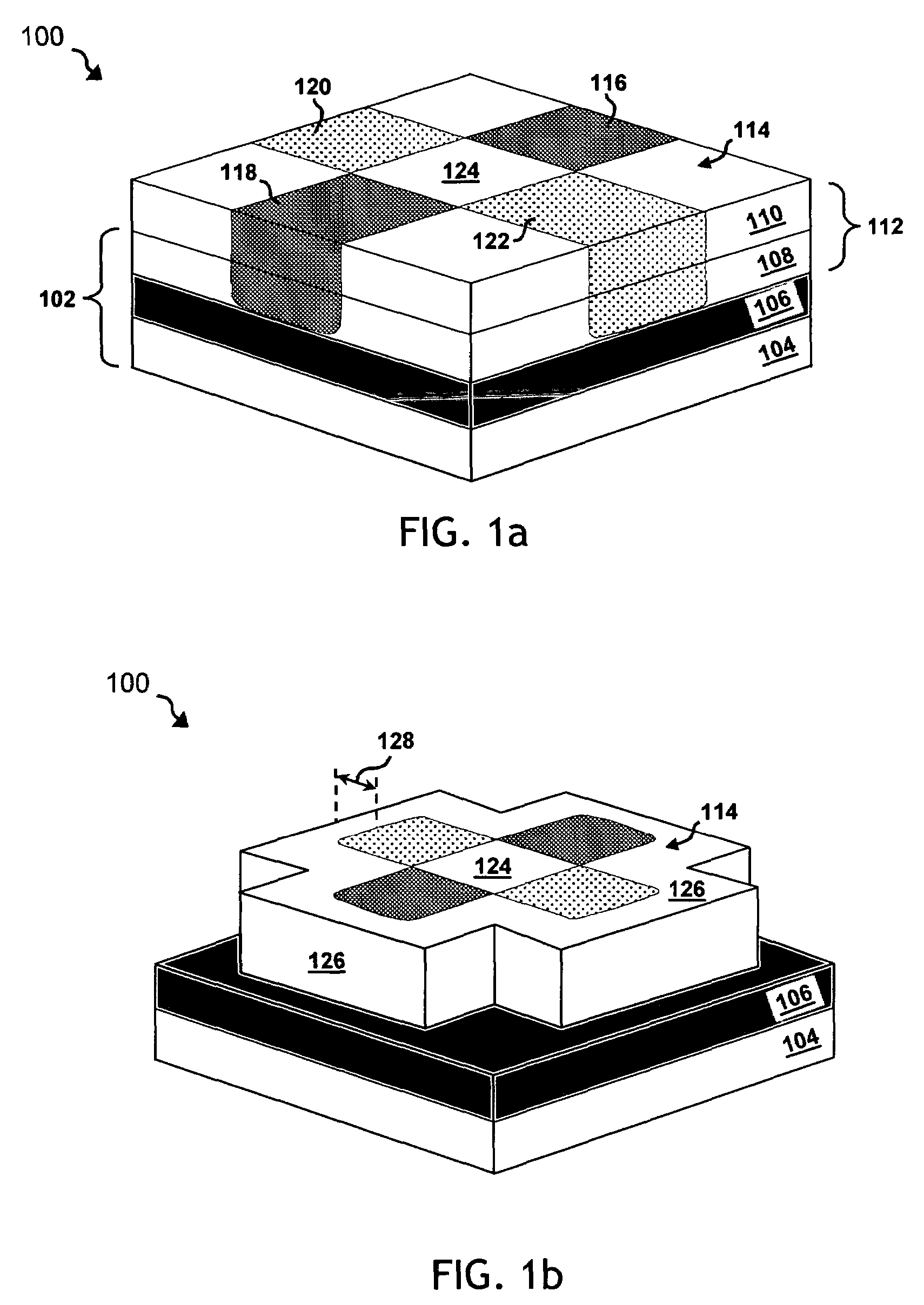
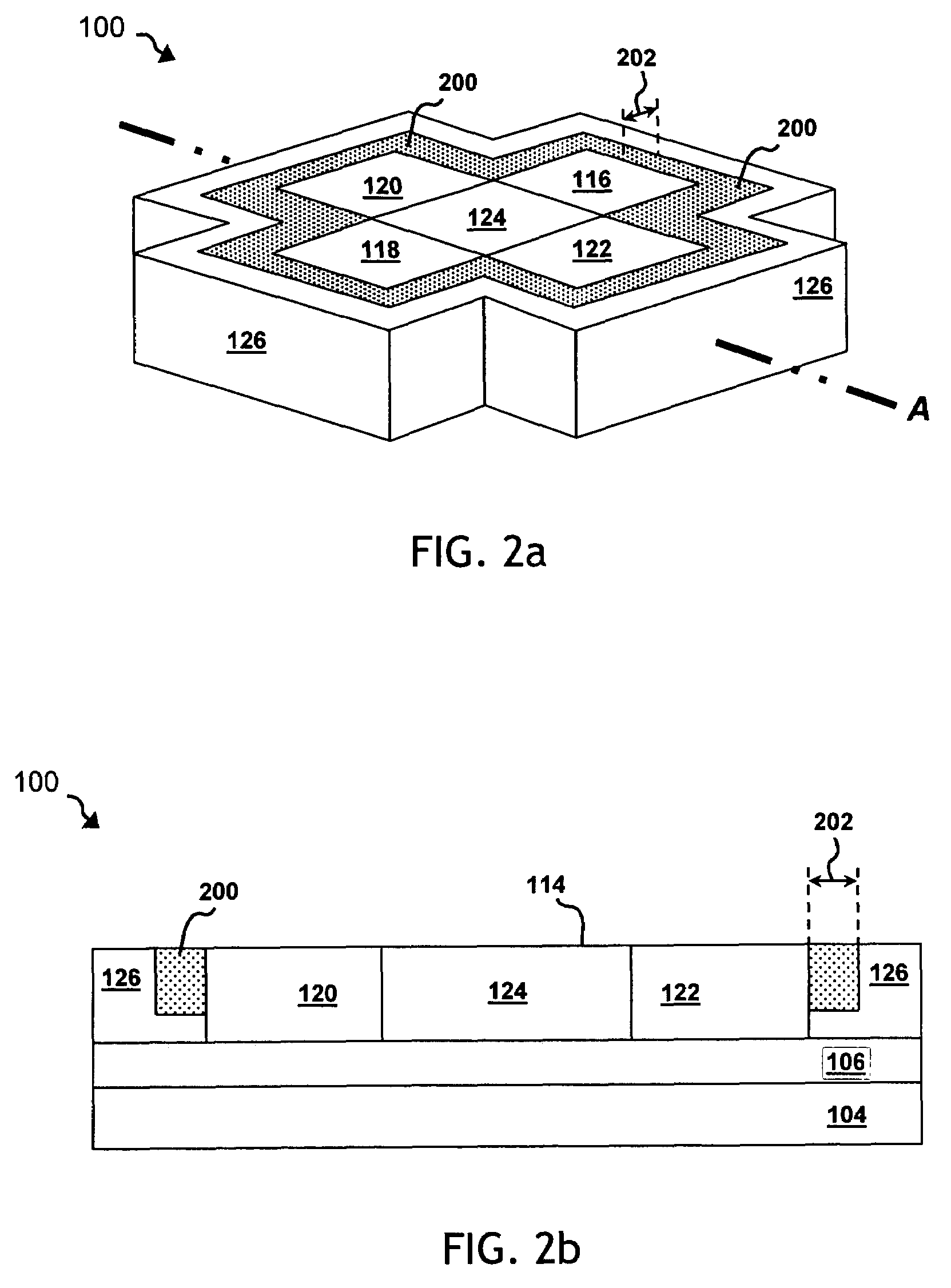
[0022]While the making and using of various embodiments of the present invention are discussed in detail below, it should be appreciated that the present invention provides many applicable inventive concepts, which can be embodied in a wide variety of specific contexts. The present invention is hereafter illustratively described in conjunction with the design and production of JFET structures utilizing a MOS-type semiconductor process technology. The specific embodiments discussed herein are, however, merely demonstrative of specific ways to make and use the invention and do not limit the scope of the invention

[0023]Comprehending a number of inefficiencies and limitations arising from conventional JFET designs, the present invention provides a versatile system for the design and production of high performance JFET structures. The present invention overcomes detrimental effects of processing imprecision during the production of certain transistor features—particularly the channel reg...


PUM


Abstract

The present invention provides a system for providing a cross-lateral junction field effect transistor (114) having desired high-performance desired voltage, frequency or current characteristics. The cross-lateral transistor is formed on a commercial semiconductor substrate (102). A channel structure (124) is formed along the substrate, having source (120) and drain (122) structures laterally formed on opposites sides thereof. A first gate structure (116) is formed along the substrate, laterally adjoining the channel structure orthogonal to the source and drain structures. A second gate structure (118) is formed along the substrate, laterally adjoining the channel structure, orthogonal to the source and drain structures and opposite the first gate structure.

Description

TECHNICAL FIELD OF THE INVENTION[0001]The present invention relates generally to the field of semiconductor devices and, more particularly, to apparatus and methods for the production of junction field effect transistors.BACKGROUND OF THE INVENTION[0002]The continual demand for enhanced integrated circuit performance has resulted in, among other things, a dramatic reduction of semiconductor device geometries, and continual efforts to optimize the performance of every substructure within any semiconductor device. A number of improvements and innovations in fabrication processes, material composition, and layout of the active circuit levels of a semiconductor device have resulted in very high-density circuit designs. Increasingly dense circuit design has not only improved a number of performance characteristics, it has also increased the importance of, and attention to, semiconductor material properties and behaviors.[0003]The increased packing density of the integrated circuit genera...

Claims


Application Information

Patent Timeline
Patent Type & Authority Patents(United States)
IPC IPC(8): H01L29/74H01L31/111
CPCH01L29/808H01L29/0692
Inventor HOWARD, GREGORY E.SWANSON, LELAND
Owner TEXAS INSTR INC
Why Eureka
Try Eureka