Electromagnetic pumping of liquid silicon in a crystal growing process

a technology of liquid silicon and crystal growth, applied in the direction of crystal growth process, polycrystalline material growth, under a protective fluid, etc., can solve the problems of increasing the mechanical strength of silicon wafers, inferior devices, non-uniformity both axially and radially, etc., to improve efficiency, flexibility, and capability

Active Publication Date: 2007-11-06
GLOBALWAFERS CO LTD
View PDF17 Cites 16 Cited by
  • Summary
  • Abstract
  • Description
  • Claims
  • Application Information

AI Technical Summary

Benefits of technology

[0013]The invention meets the above needs and overcomes one or more deficiencies in the prior art by providing a system and method for applying a time-varying magnetic field to a melt to generate pumping forces in the melt to control the melt flow during the growth process on both short-term and long-term scales. By influencing the flow of liquid silicon in the Czochralski (Cz) crystal growth process, both heat and matter transfer in the melt can be controlled, and, therefore determine the composition and properties of the crystal grown from the melt, as well as the growth process itself. Moreover, the invention provides the desired melt flow control with improved efficiency, flexibility, and capability that combine the benefits from the three conventional magnetic field configurations while providing additional advantages.

Problems solved by technology

In the various heat treatment processes during the manufacture of various electrical devices, the oxygen in the crystal may cause crystal defects such as precipitates, dislocation loops, and stacking faults or it may cause electrically active defects resulting in devices with inferior performance characteristics.
The solid solution of oxygen in the crystal, however, increases the mechanical strength of silicon wafers, and the crystal defects may improve the yield of conforming products by entrapping contaminants of heavy metals.
However, the current induced in the melt as a result of convective flow in the r-z plane produces forces in the melt that retard the melt flow which produced it.
But its non-uniformity both axially and radially and the complex and bulky setup introduce additional design consideration when applying the horizontal magnetic field configuration in large diameter Czochralski growth processes.

Method used


Image

  • Electromagnetic pumping of liquid silicon in a crystal growing process
  • Electromagnetic pumping of liquid silicon in a crystal growing process
  • Electromagnetic pumping of liquid silicon in a crystal growing process

Examples


Embodiment Construction

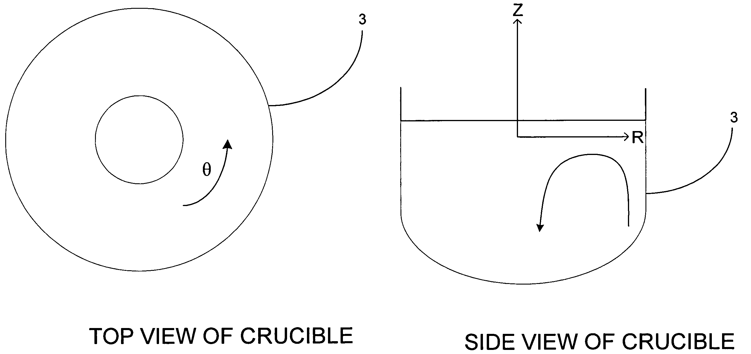
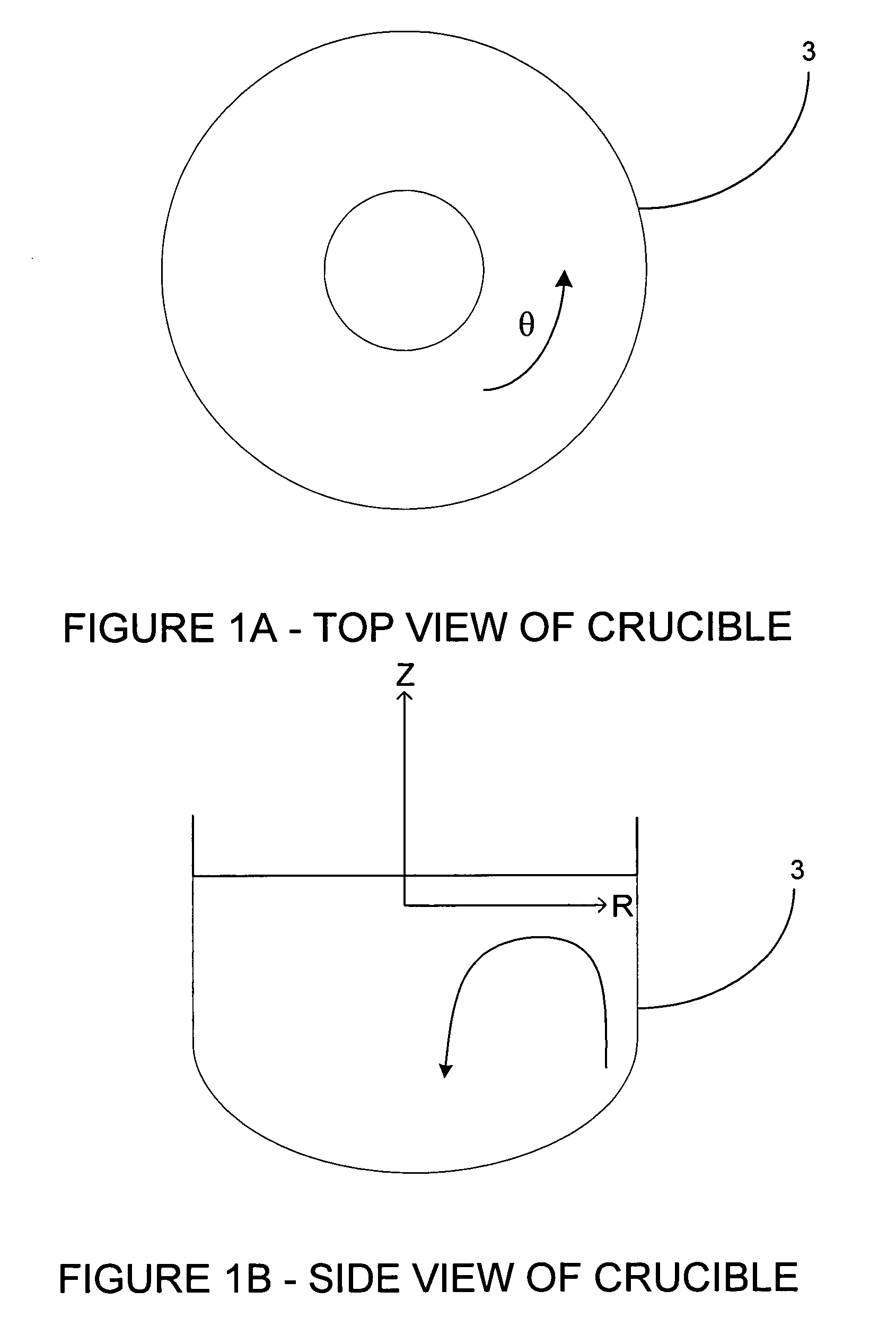
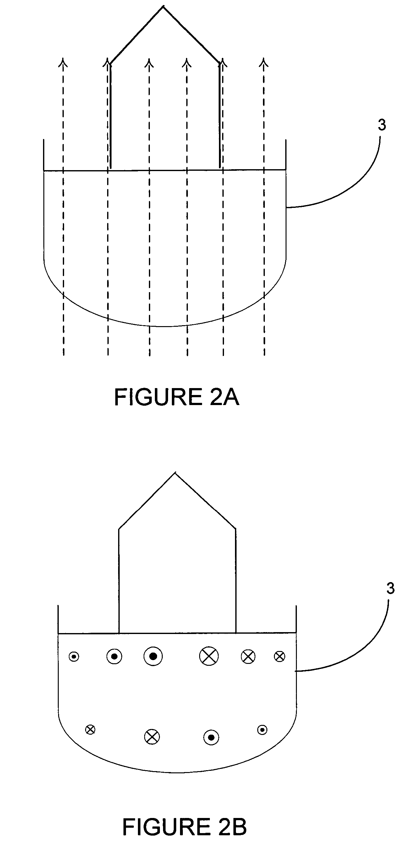
[0033]Embodiments of the present invention provide a control system that improves a global melt flow pattern in a silicon melt during a Czochralski crystal growing process. More specifically, a time-varying (i.e., dynamic) magnetic field is applied to the melt to generate upward or downward pumping forces in the melt. Advantageously, these pumping forces can be used to increase or decrease a velocity of the melt flow as desired. According to one embodiment of the invention, the control system has two modes of operation in which the pumping forces can be generated in the melt to achieve a desired effect (i.e., increase or decrease) on the melt flow velocity. In a first mode of operation, the magnetic field applied to the melt is varied for period of time and is responsive to a control parameter such as diameter to generate a pumping force in the melt that increases or decreases melt flow velocity. In a second mode of operation, the magnetic field applied to the melt can be varied thr...


PUM

PropertyMeasurementUnit
magnetic fieldaaaaaaaaaa

Abstract

A method and system for use in combination with a crystal growing apparatus for growing a monocrystalline ingot according to a Czochralski process. The crystal growing apparatus has a heated crucible including a semiconductor melt from which the ingot is pulled. The ingot is grown on a seed crystal pulled from the melt. A time varying external magnetic field is imposed on the melt during pulling of the ingot. The magnetic field is selectively adjusted to produce pumping forces in the melt to control a melt flow velocity while the ingot is being pulled from the melt.

Description

FIELD OF THE INVENTION[0001]The present invention generally relates to producing semiconductor grade single crystal silicon that can be used in the manufacture of electronic components and the like. More particularly, the present invention relates to a system and method for controlling melt flow by producing pumping forces in the melt using a time-varying magnetic field.BACKGROUND OF THE INVENTION[0002]Single crystal silicon, which is the starting material in most processes for fabricating semiconductor electronic components, is commonly prepared according to the so-called Czochralski process. In this process, polycrystalline silicon, or polysilicon, is charged to a crucible and melted, a seed crystal is brought into contact with the molten silicon, and a single crystal ingot is grown by relatively slow extraction. After formation of a neck is complete, decreasing the pulling rate and / or the melt temperature enlarges the diameter of the crystal until a desired or target diameter is ...

Claims


Application Information

Patent Timeline
Patent Type & Authority Patents(United States)
IPC IPC(8): C30B15/20
CPCC30B15/305Y10S117/917C30B15/30C30B29/06
Inventor KORB, HAROLD W
Owner GLOBALWAFERS CO LTD
Why Eureka
Try Eureka