Capacitor charging circuitry and methodology implementing controlled on and off time switching

a capacitor and charging circuit technology, applied in the direction of ac-dc conversion, secondary cell charging/discharging, electric variable regulation, etc., can solve the problems of impractical implementation of conventional power switching supplies, inability to adjust the tsub>off/sub>/tsub>on ratio, and inability to adapt to the needs of conventional switching power supplies. , to achieve the effect of fast and efficient power transfer, high degree of flexibility, and flexible and adaptabl

Inactive Publication Date: 2007-11-06
ANALOG DEVICES INT UNLTD
View PDF18 Cites 24 Cited by
  • Summary
  • Abstract
  • Description
  • Claims
  • Application Information

AI Technical Summary

Benefits of technology

[0013]This architecture may be considered current based because it determines the ON-time and the OFF-time as a result of the current through the primary and secondary windings of the transformer. This current-based switching arrangement can provide a versatile and adaptable switching topology that yields fast and efficient transfer of power to capacitive loads. In particular, both the switch-ON time and switch-OFF time can be adaptable to conditions present in the circuit. For example, the ON-time / OFF-time cycle can exhibit a high degree of flexibility in providing power to charge capacitive loads ranging from zero volts to several hundred volts. The adaptable switch topology can also adapt automatically for variations in the power supply input voltage. For example, if the input voltage is lower than average, the ON-time circuitry may not deactivate the power switch as soon as if the input voltage was relatively average. In this way, the power delivery circuitry can energize the transformer to substantially the same level even though the input voltage is lower.
[0014]The measuring circuitry of the present invention provides the capacitor charging circuit with the ability to indirectly measure the output capacitor load voltage by monitoring the voltage waveform on the primary transformer winding during the OFF-time cycle. Measuring the voltage on the primary transformer winding during the OFF-time cycle can provide the capacitor charging circuit with the ability to reduce wasteful power consumption.

Problems solved by technology

This approach as it relates to photoflash systems, however, has several potential problems.
One problem is that the photoflash capacitor voltage can vary continuously from, for example, 0V at the start of a charging cycle to 300V at the end of the charging cycle.
This wide variation in voltages can put demands that are impractical to implement on conventional power switching supplies.
For example, some conventional switching power supplies may not have the capability to adjust the TOFF / TON ratio to provide power to charge output capacitor loads that vary over a wide voltage range.
Another potential problem that may occur with conventional power switching supplies is that the output voltage feedback mechanism used to monitor the output voltage can be a source of constant power dissipation.
During operation, this coupling exhibits an I2R power loss.
In addition, when the conventional switching supply operates to maintain a relatively high output voltage (e.g., 300V), the feedback mechanism can dissipate several milliwatts.
Since it is desirable to maintain the capacitor voltage at flash ready status, the feedback mechanism has to constantly monitor the capacitor voltage to ensure that the proper voltage is maintained, thus creating an undesirable long term power loss.
Another problem that can occur with conventional switching power supplies is that the switching action required to obtain the proper output voltage cannot be stopped.
This can add additional power losses that reduce the efficiency of conventional photoflash systems.

Method used


Image

  • Capacitor charging circuitry and methodology implementing controlled on and off time switching
  • Capacitor charging circuitry and methodology implementing controlled on and off time switching
  • Capacitor charging circuitry and methodology implementing controlled on and off time switching

Examples


Embodiment Construction

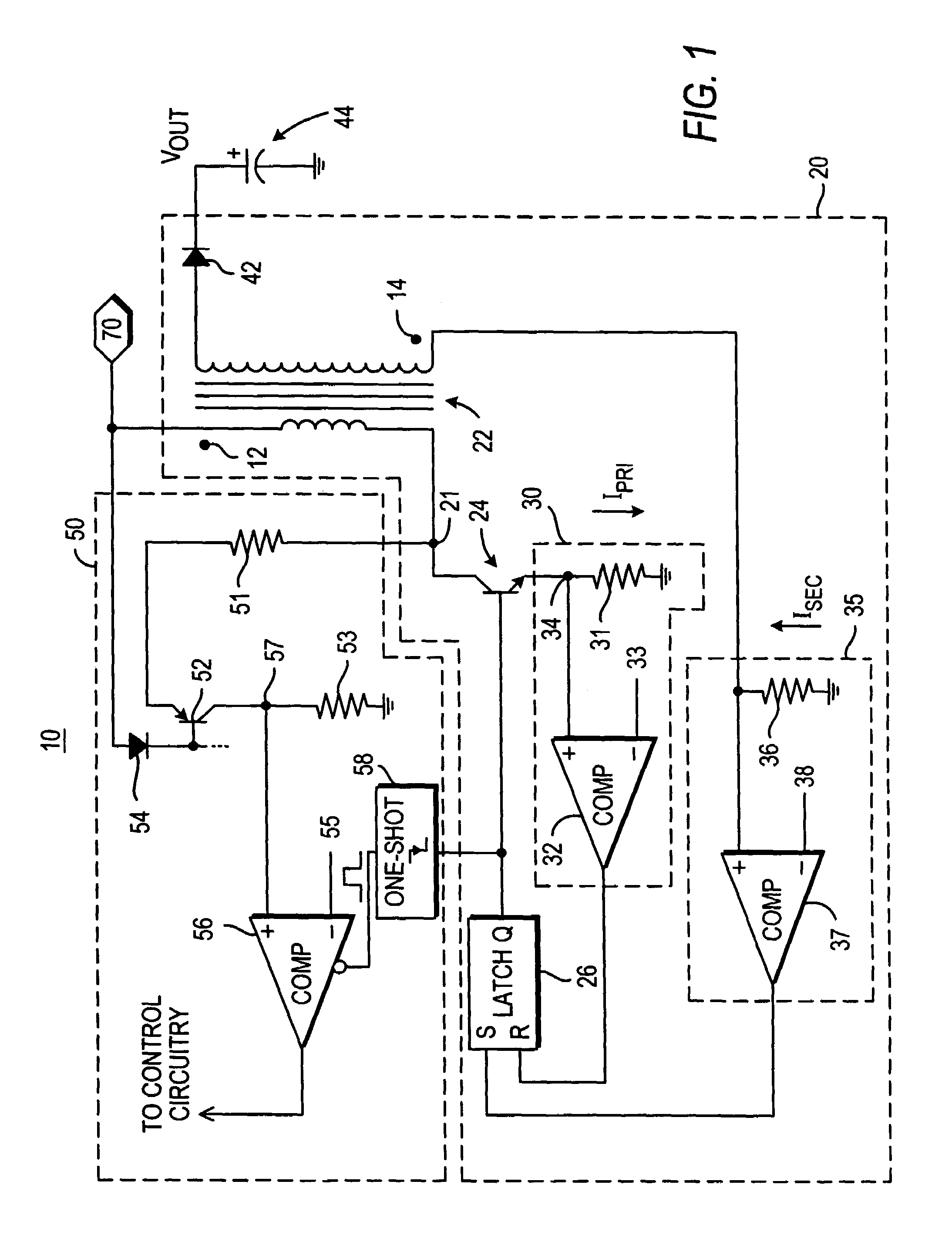
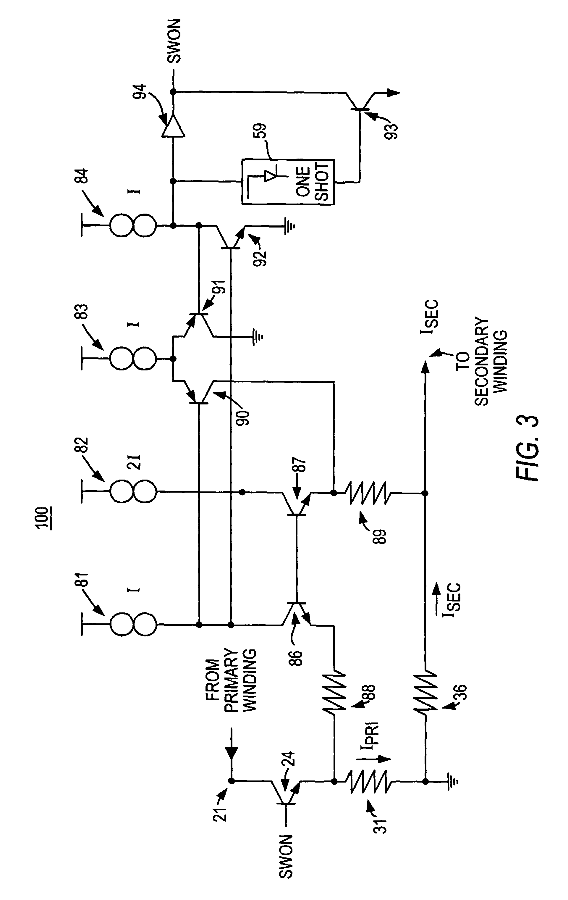
[0028]Circuits and techniques for providing high efficiency charging of capacitive loads are provided. In particular, circuits and techniques are provided for charging capacitive loads in photoflash systems.

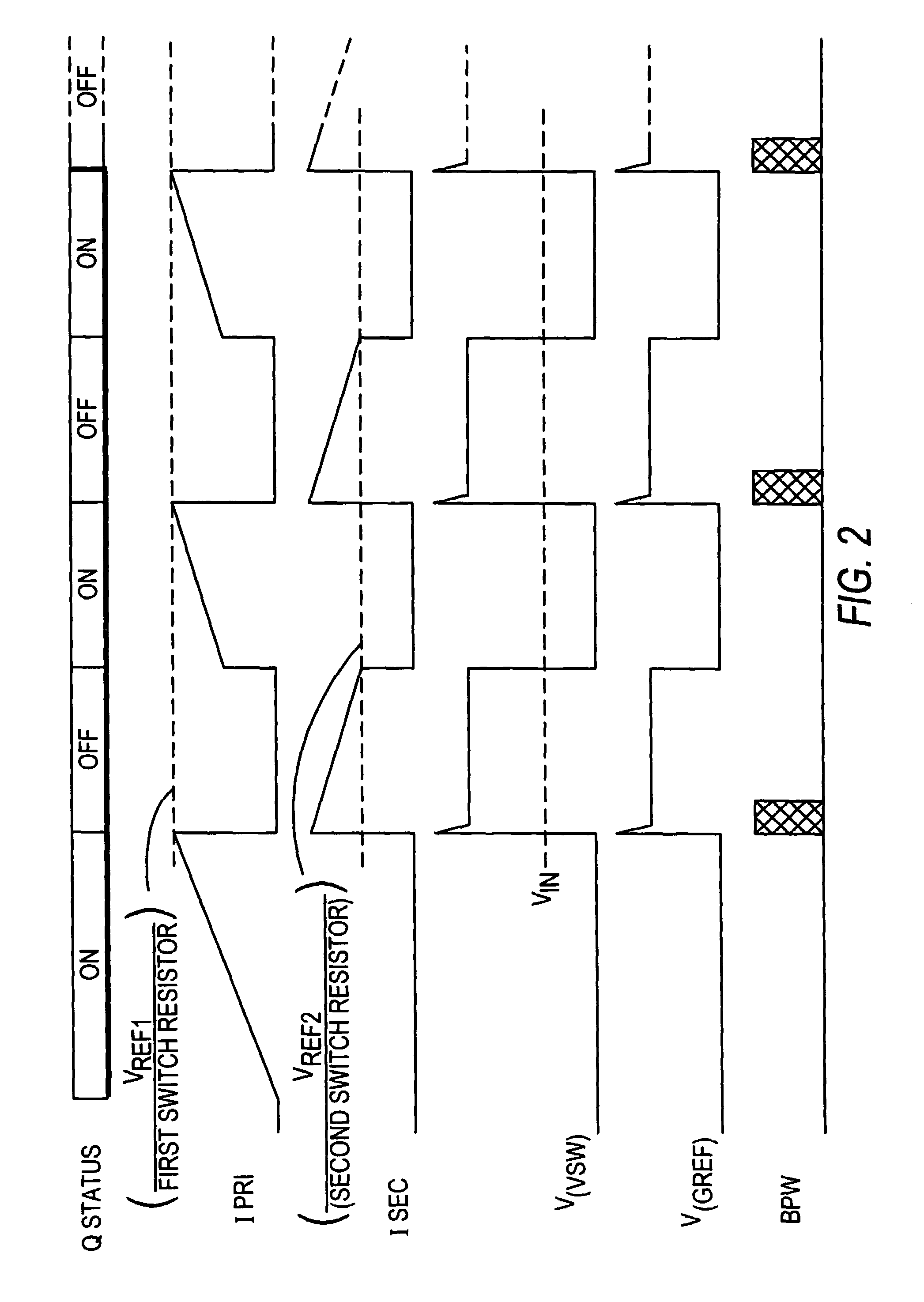
[0029]In conventional photoflash capacitor charging circuits, conventional switching power supplies may be implemented to charge an output capacitor to a desired output voltage. The conventional switching power supply may charge the output capacitor by adjusting the TOFF / TON ratio of the switching cycle to obtain the desired output voltage.

[0030]However, conventional photoflash capacitor charging circuits present a number of potential problems, as described above. The conventional capacitor charging circuit may measure the output voltage using a resistor divider, which can produce an undesirable power loss. Other problems may involve the inability of the conventional switching power supply to efficiently charge a capacitive load for continuously varying output voltages. A photofl...


PUM

PropertyMeasurementUnit
voltageaaaaaaaaaa
output voltageaaaaaaaaaa
voltageaaaaaaaaaa

Abstract

The present invention provides a capacitor charging circuit that efficiently charges capacitive loads. In particular, circuits and techniques are preferably provided for using current from both the primary and secondary windings of a transformer to control ON-time and OFF-time of a switch. This arrangement preferably yields an adaptable ON-time and adaptable OFF-time switch that is capable of rapidly charging capacitor loads ranging from as low as zero volts to several hundred volts. The output voltage is preferably measured indirectly to prevent unnecessary power consumption. In addition, control circuitry can be provided to conserve power by ceasing the delivery of power to the capacitor load once the desired output voltage is reached. Control circuitry preferably operates an interrogation timer that periodically activates the power delivery cycle to maintain the capacitor output load in a constant state of readiness.

Description

CROSS-REFERENCE TO A RELATED PATENT APPLICATION[0001]This is a continuation-in-part of U.S. patent application Ser. No. 10 / 324,628, filed Dec. 18, 2002, which is a continuation of U.S. patent application Ser. No. 09 / 921,466, filed Aug. 3, 2001, now U.S. Pat. No. 6,518,733, both of which are hereby incorporated by reference herein in their entirety.BACKGROUND OF THE INVENTION[0002]This invention relates to charging capacitive loads. More particularly, this invention relates to charging capacitive loads in photoflash systems.[0003]In conventional photoflash systems, fixed frequency switching power supply topologies are typically used to provide power to a capacitive load. For example, in fixed frequency applications, a portion of the period associated with the frequency can be used to turn a power switch (e.g., transistor) ON and another portion of the period can be used to turn the switch OFF. A ratio of ON-time TON versus OFF-time TOFF can be set to adjust the duty ratio applied to ...

Claims


Application Information

Patent Timeline
Patent Type & Authority Patents(United States)
IPC IPC(8): H01M10/44H01M10/46H02J7/10H02J1/00H02M3/28H02M3/335H02M3/338H05B41/30
CPCH02M3/335H05B41/30H02M3/3385H02M3/33507
Inventor PIETKIEWICZ, STEVEN MWU, ALBERT M
Owner ANALOG DEVICES INT UNLTD
Why Eureka
Try Eureka