Process for producing polymer optical waveguide and resin injecting device

a technology of optical waveguide and resin injection, which is applied in the direction of instruments, optical elements, other domestic objects, etc., can solve the problems of process cost, increase in cost, and inability to provide a sufficient refraction index difference between the core layer, etc., to achieve high precision level, reduce the loss of guided waves, and high productivity

Inactive Publication Date: 2007-11-13
FUJIFILM BUSINESS INNOVATION CORP
View PDF25 Cites 13 Cited by
  • Summary
  • Abstract
  • Description
  • Claims
  • Application Information

AI Technical Summary

Benefits of technology

[0018]In light of the above-mentioned problems, the present invention has been completed. An object thereof is to provide a process for producing a polymer optical waveguide in which the shape of a core thereof is kept at a high precision level to reduce loss of guided waves, with a high productivity, in a simple manner. Moreover, the another object of the invention is to provide a resin injecting device which can be used in the above-described process.
[0021]The above-mentioned mold is used in the process for producing a polymer optical waveguide of the invention. Therefore, even if the core-forming curable resin is injected into the concave portion in the mold under pressure, the mold does not deform or the mold and the cladding substrate are not shifted from predetermined positions thereof. As a result, the filling speed can be increased without sacrificing the precision of the core shape. Thus, according to the production process of the invention, a polymer optical waveguide wherein the shape of a core thereof is kept at a high precision level to reduce loss of guided waves can be produced with a high productivity in a simple manner.

Problems solved by technology

However, the selective polymerization process (1) has a problem with regard to the sticking of the film, and the processes (2) and (3) result in an increase in costs since photolithography is used.
The process (4) has a problem with regard to precision of the resultant core diameter, and the process (5) cannot provide a sufficient refraction index difference between the core layer and the clad layer.
However, these processes also have a problem with regard to costs as described above.
Therefore, light leaks out through this thin layer.
However, because of the use of the monomer as the core forming material in this method, a volume shrinkage ratio of the monomer is large when the monomer is polymerized.
Consequently, transmission loss of the polymer optical waveguide becomes large.
This method is also a complicated method, in which the pattern substrate and the flat substrate are fixed to each other with the clamp, and the contacting portion is sealed with the resin.
Thus, this method is not suitable for mass production.
As a result, a reduction in costs cannot be expected.
Moreover, this method cannot be applied to the production of a polymer optical waveguide using, as a clad, a film having a thickness on the order of several millimeters or a thickness of 1 mm or less.
However, even if the production process described in this patent is applied to the production of a polymer optical waveguide, it takes much time to form a core portion thereof since a sectional area of the core portion of the optical waveguide is small.
Thus, the process is unsuitable for mass production.
This process also has a drawback in that when a monomer solution is polymerized, a volume change is caused, so that a shape of the core is also changed, and consequently transmission loss becomes large.
However, when an optical waveguide is formed by a micromolding method as described above, reduction of the volume shrinkage ratio of a polymer (so that transmission loss is reduced) when the polymer is cured is incompatible with reduction of the viscosity of a filling liquid (the monomer and so forth) in order to attain easy filling.
Accordingly, in a case where reduction of transmission loss is preferentially considered, the viscosity of the filling liquid cannot be lowered sufficiently and a filling speed becomes slow.
Thus, the mass production of optical waveguides by this method cannot be expected.
Thus, use of a flexible film substrate in this method has not been considered in this method.

Method used


Image

  • Process for producing polymer optical waveguide and resin injecting device
  • Process for producing polymer optical waveguide and resin injecting device
  • Process for producing polymer optical waveguide and resin injecting device

Examples


example 1

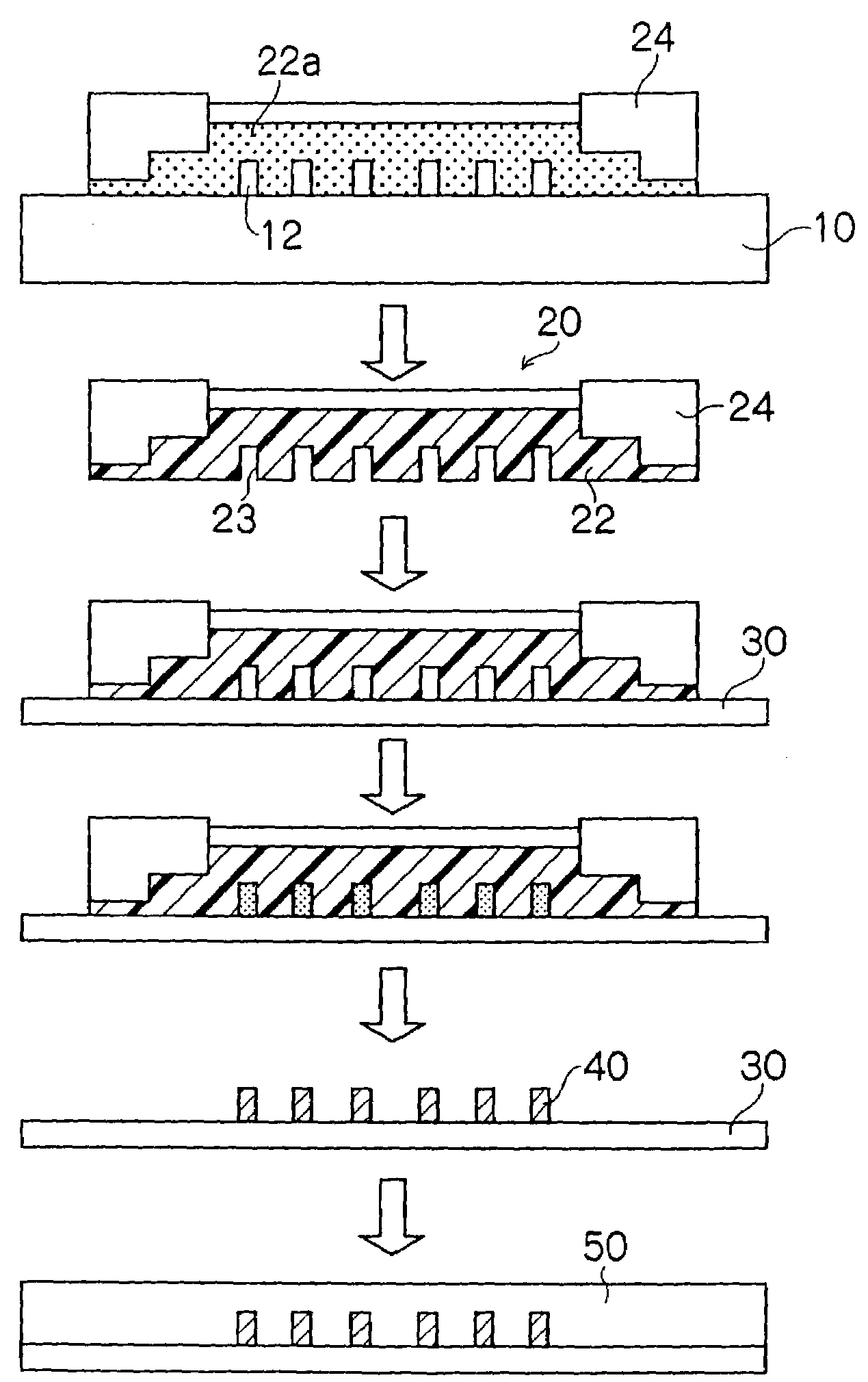
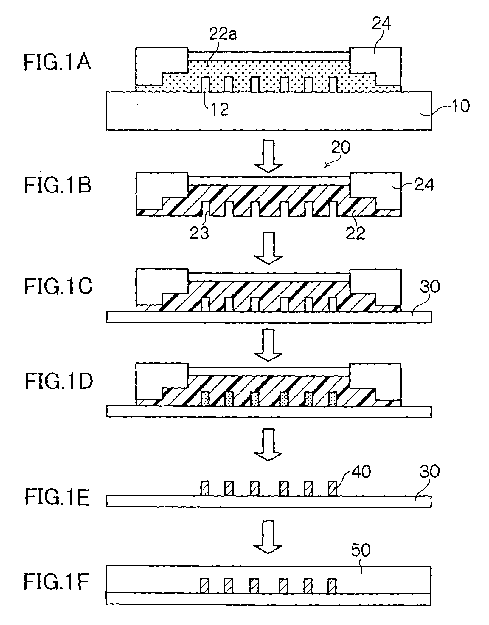
[0081]An ultraviolet curable thick film resist solution (SU-8, made by MicroChem. Corp.) was applied to a Silicon monocrystal substrate by spin-coating, and then the resultant layer was pre-baked in a heating oven at 80° C. The resultant was exposed through a photo mask to light from a high-pressure mercury lamp, and developed, so as to form a substrate having fine convex portions having a square section (width: 50 μm, height: 50 μm, and length: 60 mm). Next, this was post-baked at 120° C. to form a master template for producing optical waveguide cores.

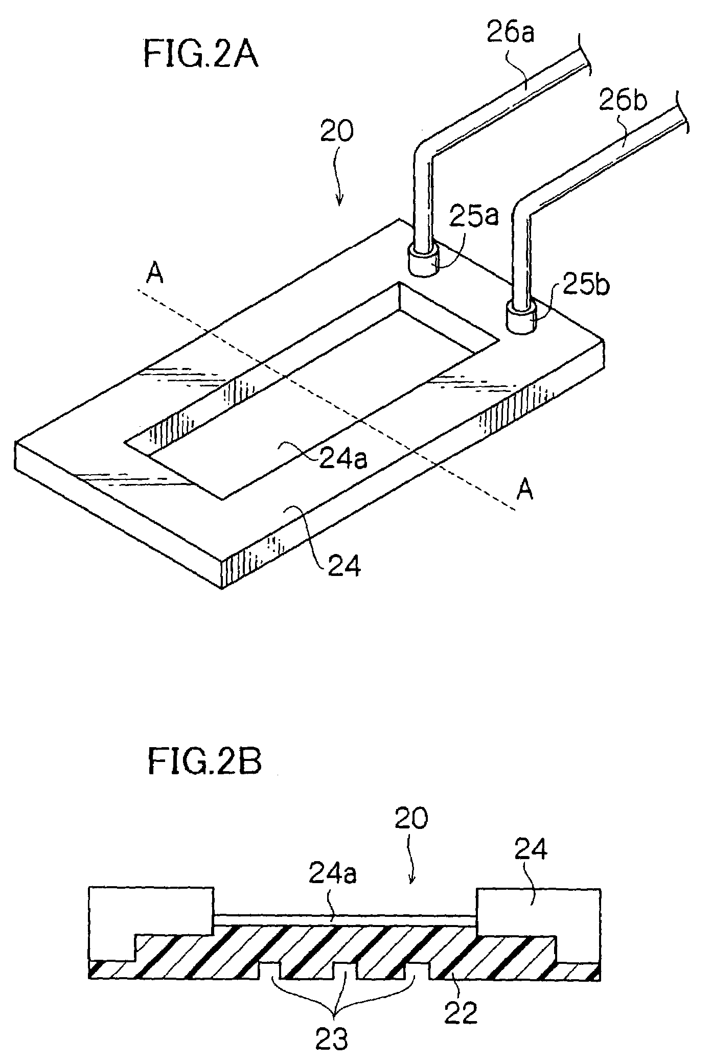
[0082]Next, a reinforcing member as illustrated in FIGS. 2A and 2B was formed. An opening 24a for light exposure was made of quartz.

[0083]A releasing agent was applied to the master template, and then a thermosetting silicone rubber oligomer (dimethylpolysiloxane SYLGARD 184, made by Dow Corning Asia Ltd.) was applied onto the master template, as illustrated in FIG. 5A. The reinforcing member was pressed onto the silicone rubber oligo...

example 2

[0087]A polymer optical waveguide was produced in the same manner as in Example 1 except that a reinforcing member having injection inlets and air outlets as illustrated in FIG. 4 was used instead of the reinforcing member in Example 1; the internal pressure of the mold (the space V2 in FIG. 5C) was reduced through the pressure-reduction exhaust pipe at the same time when the core-forming curable resin was injected under pressure; an ultraviolet ray-curable resin (made by JSR Corp., refractive index: 1.500) having a viscosity of 500 mPa·s was used as the core-forming curable resin; and the ultraviolet ray-curable resin was cured by UV having an intensity of 75 mW / cm2. The loss of this polymer optical waveguide was 0.41 dB / cm.

example 3

[0088]Using a glass substrate, a master template was formed in the same manner as in Example 1. The same mold as used in Example 2 was formed.

[0089]This mold was brought into close contact with an Arton film (made by JSR Corp., refractive index: 1.510) having a thickness of 188 μm. An ultraviolet ray-curable resin (PJ3001, made by JSR Corp.) having a viscosity of 1300 mPa·s, which was a core-forming curable resin, was injected from the injection pipe to concave portions in the mold under pressure. At this time, the pressure in the concave portions was reduced and the air was removed from the other end of the mold. After the ultraviolet ray-curable resin filled the concave portions in the mold, the injection pipe and the pressure-reduction exhaust pipe were removed from the mold and then UV light having an intensity of 50 mW / cm2 was radiated through the opening for light exposure of the mold onto the resin for 10 minutes, so as to cure the resin in the concave portions. The mold was ...


PUM

PropertyMeasurementUnit
thicknessaaaaaaaaaa
thicknessaaaaaaaaaa
surface energyaaaaaaaaaa

Abstract

The present invention provides a process for producing a polymer optical waveguide, comprising the steps of: preparing a mold comprising a concave portion; bringing a substrate into contact with the mold, filling the concave portion with a core-forming curable resin; curing the core-forming curable resin in the concave portion; removing the mold from the substrate; and forming a clad layer on the substrate; wherein the mold comprises a cured resin layer and a reinforcing member, the cured resin layer has the concave portion, the reinforcing member has an introduction portion which communicates with the concave portion and an injection inlet which communicates with the introduction portion, and a discharge portion which communicates with the concave portion is provided in the reinforcing member, the cured resin layer and / or a space between the cured resin layer and the reinforcing member, and a resin injecting device which is used in the process.

Description

BACKGROUND OF THE INVENTION[0001]1. Field of the Invention[0002]The present invention relates to a process for producing an optical waveguide, in particular, a flexible polymer optical waveguide, and to a resin injecting device.[0003]2. Description of the Related Art[0004]As a process for producing a polymer optical waveguide, the following processes are suggested: (1) a process of impregnating a film with a monomer, selectively exposing a core portion to light to change a refraction index thereof, and sticking a film thereto (selective polymerization); (2) a process of applying a core layer and a clad layer to a substrate, and forming a clad portion by reactive ion etching (RIE); (3) a process using photolithography, in which an ultraviolet ray-curable resin obtained by adding a photosensitive material to a polymer is imagewise exposed to light and developed (direct exposure); (4) an injection molding process and; (5) a process of applying a core layer and a clad layer to a substra...

Claims


Application Information

Patent Timeline
Patent Type & Authority Patents(United States)
IPC IPC(8): B29D11/00G02B6/13B29C33/00B29C33/10B29C33/38B29C33/40B29C35/08B29C39/26G02B6/12G02B6/122G02B6/138
CPCB29C33/3857B29C39/26B29D11/00663G02B6/1221G02B6/138B29C33/0077B29C33/10B29C33/405G02B2006/121B29C35/0888
Inventor AKUTSU, EIICHIOHTSU, SHIGEMISHIMIZU, KEISHIYATSUDA, KAZUTOSHI
Owner FUJIFILM BUSINESS INNOVATION CORP
Why Eureka
Try Eureka