Method of manufacturing electrode for secondary cell

Inactive Publication Date: 2007-11-13
SANYO ELECTRIC CO LTD
View PDF13 Cites 0 Cited by
  • Summary
  • Abstract
  • Description
  • Claims
  • Application Information

AI Technical Summary

Benefits of technology

[0010]An object of the present invention is to provide a method of manufacturing an electrode for a secondary cell capable of readily forming an active material layer only on a necessary portion of a collector by a method supplying raw material from a gas phase.

Problems solved by technology

If the active material layer is present between the tab and a collector, therefore, a cell characteristic such as the cell voltage is disadvantageously reduced when the active material layer itself has low electric conductivity.
However, the active material layer formed by sputtering or the like has large adhesion to the collector.
Therefore, it is difficult to partially mechanically separate the active material layer formed on the overall surface of the collector from the portion of the collector requiring no active material layer.
Thus, in the conventional method of forming an active material layer on a collector by a method such as sputtering supplying raw material from a gas phase, it is disadvantageously difficult to partially remove the active material layer formed on the overall surface of the collector from the portion of the collector requiring no active material layer, and it is consequently difficult to locate the active material layer only on a necessary portion of the collector.

Method used


Image

  • Method of manufacturing electrode for secondary cell
  • Method of manufacturing electrode for secondary cell
  • Method of manufacturing electrode for secondary cell

Examples


example 1

[0041]Example 1 of the present invention is described with reference to mask layers consisting of styrene-butadiene rubber (SBR) reduced in adhesion to a collector due to a high temperature for forming active material layers when forming a negative electrode of a lithium secondary cell.

[0042][Preparation of Negative Electrode]

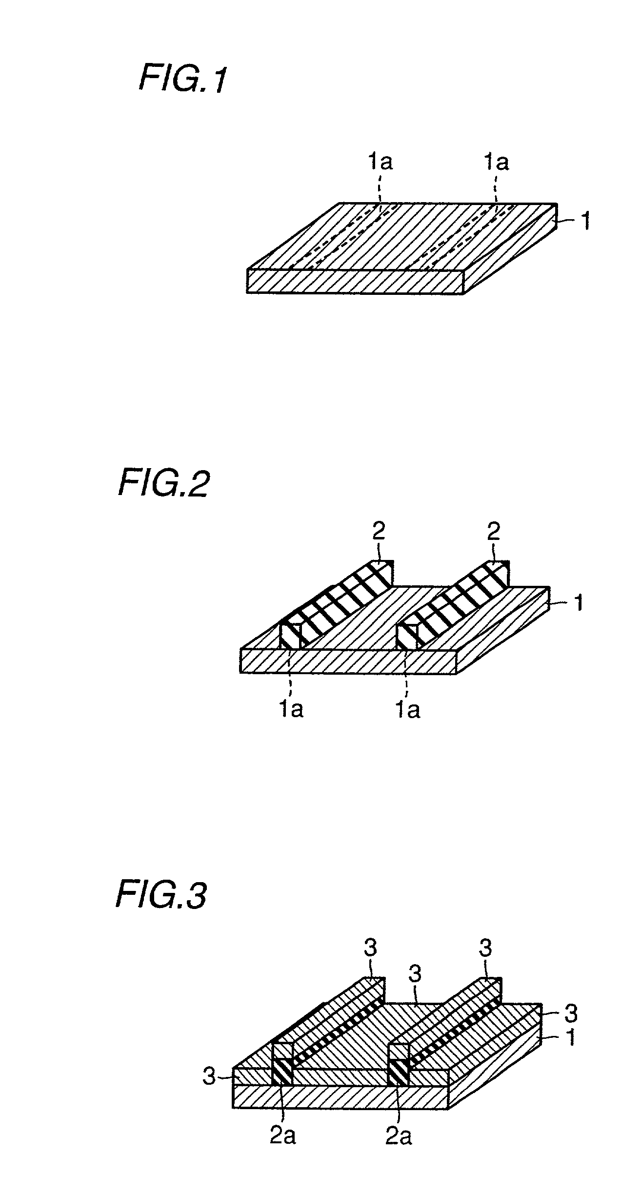
[0043]Before describing actual conditions for preparing a negative electrode according to Example 1, the process of preparing the negative electrode is conceptually described with reference to FIGS. 1 to 4. According to Example 1, a collector 1 is first prepared as shown in FIG. 1. Then, regions 1a requiring formation of no active material layers such as tab portions etc. are specified on the surface of the collector 1. As shown in FIG. 2, mask layers 2 consisting of a material reduced in adhesion to the collector 1 due to a high temperature for forming active material layers 3 (see FIG. 3) described later are formed on the regions 1a of the collector 1 requiri...

example 2

[0057]Example 2 of the present invention is described with reference to resist layers employed as mask layers formed on a collector in preparation of a negative electrode. More specifically, the overall surface of a previously electrolyzed electrolytic copper foil member having a thickness of 20 μm forming a collector was electrodeposition-coated with a liquid emulsion mainly composed of a copolymer of methyl methacrylate, n-butyl acrylate and methacrylic acid, thereby forming resist layers (PHOTO-ED P5000 by Nippon Paint Co., Ltd.) in a thickness of 20 μm. Thereafter exposure and development were performed for forming mask layers consisting of the resist layers having patterns similar to those in Example 1. Active material layers consisting of amorphous silicon layer having a thickness of about 6 μm were formed on the collector consisting of the electrolytic copper foil member and on the mask layers by sputtering. The amorphous silicon layers were formed under conditions of power (...

example 3

[0061]Example 3 of the present invention is described with reference to heat-resistant tapes consisting of polyimide resin employed as mask layers for preparing a negative electrode. According to Example 3, heat-resistant tapes of polyimide resin having a thickness of about 60 μm were applied onto a collector consisting of a previously electrolyzed electrolytic copper foil member having a thickness of 20 μm in the same patterns as those shown in Example 1. An active material layer consisting of amorphous silicon was formed on the overall surface of the electrolytic copper foil member (collector) having the heat-resistant tapes of polyimide resin applied thereto in a thickness of 6 μm by sputtering under the same conditions as those in Example 1. When the heat-resistant tapes of polyimide resin were thereafter separated, the surface of the electrolytic copper foil member requiring formation of no active material layers could be exposed. The remaining parts of the amorphous silicon la...


PUM


Abstract

A method of manufacturing an electrode for a secondary cell capable of readily forming an active material layer only on a necessary portion of a collector by a method supplying raw material from a gas phase is obtained. This method of manufacturing an electrode for a secondary cell comprises steps of forming a mask layer containing a material reduced in adhesion to a collector due to a high temperature for forming an active material layer on a prescribed region of the collector, forming the active material layer on the collector and on the mask layer by a method supplying raw material from a gas phase and removing the mask layer and part of the active material layer formed on the mask layer. Thus, the mask layer is readily separated from the collector after the active material layer is formed by the method supplying raw material from a gas phase. Consequently, the mask layer and part of the active material layer formed on the mask layer are so readily removed that the active material layer is readily located only on a necessary portion of the collector.

Description

BACKGROUND OF THE INVENTION[0001]1. Field of the Invention[0002]The present invention relates to a method of manufacturing an electrode for a secondary cell, and more particularly, it relates to a method of manufacturing an electrode for a secondary cell by forming an active material layer on a collector by a method supplying raw material from a gas phase.[0003]2. Description of the Prior Art[0004]A secondary cell is recently utilized in various fields related to electronic devices and the like. In particular, a lithium secondary cell is watched with interest as a new cell having a high output and high energy density. Various types of such lithium secondary cells are developed in general.[0005]In relation to formation of an electrode active material in such a secondary cell, generally known is a technique of forming an active material layer on a collector by a method such as sputtering supplying raw material from a gas phase.[0006]A conventional electrode for a secondary cell is ins...

Claims


Application Information

Patent Timeline
IPC IPC(8): B05D5/12H01M4/139H01M6/10H01M50/531
CPCH01M2/26H01M4/04H01M4/0402H01M4/0421H01M4/0404Y02E60/122H01M6/10H01M10/05Y02E60/10H01M50/531
Inventor JITO, DAIZOTARUI, HISAKI
Owner SANYO ELECTRIC CO LTD
Why Eureka
Try Eureka