Method and system for reducing static leakage current in programmable logic devices

a programmable logic and static leakage current technology, applied in the direction of pulse technique, instruments, computation using denominational number representation, etc., can solve the problems of large number of resources available on the plds that may remain unused, stay in static mode, static power consumption to increase, etc., to reduce the power consumption of the pll/dll, reduce the static leakage, and reduce the power consumption of the phase/digital locked loop

Inactive Publication Date: 2007-11-13
ALTERA CORP
View PDF10 Cites 41 Cited by
  • Summary
  • Abstract
  • Description
  • Claims
  • Application Information

AI Technical Summary

Benefits of technology

[0005]In one aspect of the invention, a method for applying a sleep mode to components of a programmable logic device (PLD), is provided. Once it is determined that the component of the PLD or the entire PLD is non-active, a number of operations occur to reduce the static leakage. One such operation is lowering the power supply to the PLD to a minimum so that the contents within storage elements of the PLD will not be lost. The method further includes reducing the power consumption of phase/digital locked loops on the PLD. Reducing the power consumption of the PLL/DLL includes terminating power supplied to the PLL/DLL and gating...

Problems solved by technology

Consequently, a large number resources available on the PLDs may remain unused and stay in stat...

Method used


Image

  • Method and system for reducing static leakage current in programmable logic devices
  • Method and system for reducing static leakage current in programmable logic devices
  • Method and system for reducing static leakage current in programmable logic devices

Examples


Embodiment Construction

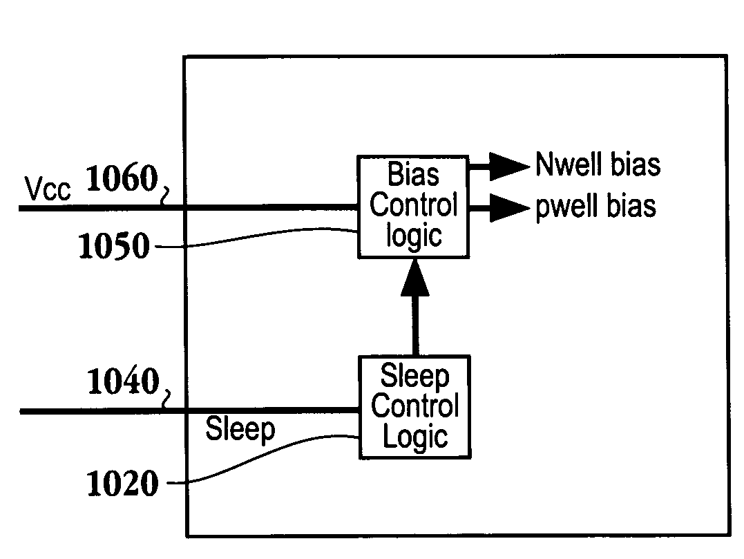
[0026]An invention for reducing static leakage current is provided. The embodiments of the present invention reduce power consumption by entering the sleep and standby mode when the device is inactive. It will be obvious, however, to one skilled in the art, that the present invention may be practiced without some or all of these specific details. In other instances, well known process operations have not been described in detail in order not to unnecessarily obscure the present invention.

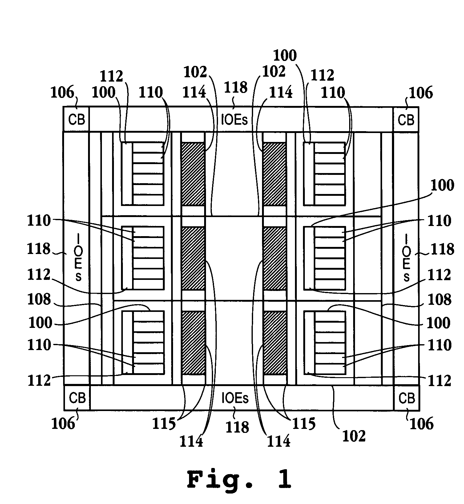
[0027]FIG. 1 is a simplified schematic diagram of the layout of a programmable logic device (PLD), in accordance with an embodiment of the invention. In one embodiment, the PLD is a Field programmable gate array (FPGA). One skilled in the art will understand and appreciate that other types of PLDs may be used in place of FPGAs. The layout includes input / output circuitry blocks (IOEs) 118, logical array blocks 100, horizontal interconnects 102, vertical interconnects 108, control blocks 106, embedded...


PUM


Abstract

A programmable logic device having logic block that can be selectively placed in a reduced power consumption mode is provided. The PLD includes a plurality of logic array blocks (LABs) and a plurality of interconnects defining signal pathways between the plurality of LABs. Sleep control logic of the PLD issues a sleep control signal for placing at least a portion of the plurality of LABs in a sleep mode. Bias control logic of the PLD is in communication with the sleep control logic. The bias control logic is triggered by the sleep control signal to issue a first bias control signal and a second bias control signal. The first and second bias control signals are transmitted to corresponding transistors of the LABS. The first and second bias control signals apply a reverse bias to corresponding transistor wells to increase threshold voltages for the respective transistors.

Description

BACKGROUNDDescription of the Related Art[0001]As the demand for smaller and faster devices increases, the manufacturers of integrated circuits (IC) are continuing to strive to decrease the feature sizes while increasing the speed, logic and memory densities. Currently, the IC technology is being scaled to sub-micron levels where the device feature sizes are reaching 65 nanometer and below in geometries. The IC device dimensions have reached a critical juncture where static leakage current or power consumption is becoming a significant portion of the overall device power.[0002]Even though static leakage power consumption is a major stumbling block for the whole semiconductor industry, this is especially important for the manufacturers of programmable logic devices (PLDs) as the PLDs provide storage, logic and wires in a standard package that can be programmed by the user according to the specification of the user. Consequently, a large number resources available on the PLDs may remai...

Claims


Application Information

Patent Timeline
IPC IPC(8): H03K19/173
CPCH03K19/17728H03K19/17784H03K19/17772
Inventor ZAVERI, KETAN H.LANE, CHRISTOPHER F.
Owner ALTERA CORP
Why Eureka
Try Eureka