Input impedance matching circuit for low noise amplifier

a low noise amplifier and input impedance matching technology, which is applied in the direction amplifiers with min 3 electrodes or 2 pn junctions, pulse techniques, etc., can solve the problems of degradation of noise figures and difficulty in implementing impedance matching low noise amplifiers, and achieve the effect of improving the gain and noise figures of low noise amplifiers

Inactive Publication Date: 2007-11-20
SAMSUNG ELECTRONICS CO LTD
View PDF12 Cites 8 Cited by
  • Summary
  • Abstract
  • Description
  • Claims
  • Application Information

AI Technical Summary

Benefits of technology

[0013]Example embodiments of the present invention provide a low noise amplifier in which parasitic capacitance at a receiving end of the low noise amplifier is used for input impedance matching of the low noise amplifier so that impedance matching may be easily performed and both gain and noise figures of the low noise amplifier may be improved.
[0014]In some embodiments of the present invention, there is provided an input impedance matching circuit for a low noise amplifier that includes a source pad, a gate pad, an input transistor, a source degeneration inductor and a matching capacitor. The gate pad receives an input signal and the input transistor amplifies the input signal transmitted from the gate pad. The source degeneration inductor coupled to an external ground voltage is adapted for input impedance matching of the low noise amplifier. The source pad is coupled to a source electrode of the input transistor and the matching capacitor is formed between the gate pad and the source pad by extending the source pad to be disposed under the gate pad. Accordingly, impedance matching of the low noise amplifier may be facilitated and the gain and noise figure of the low noise amplifier may be improved.

Problems solved by technology

However, when a degeneration inductor is used for impedance matching of a low noise amplifier, noise figure may be deteriorated due to parasitic capacitance of an electrostatic discharge protection circuit and a bonding pad of the low noise amplifier so that implementing an impedance matching low noise amplifier becomes difficult.
Moreover, the parasitic capacitance may lower the gain of the low noise amplifier and result in degradation of the noise figure.

Method used


Image

  • Input impedance matching circuit for low noise amplifier
  • Input impedance matching circuit for low noise amplifier
  • Input impedance matching circuit for low noise amplifier

Examples


Embodiment Construction

[0031]Hereinafter, the present invention will be explained in detail with reference to the accompanying drawings.

[0032]It will be understood that when an element is referred to as being “connected” or “coupled” to another element, it can be directly connected or coupled to the other element or intervening elements may be present. In contrast, when an element is referred to as being “directly connected” or “directly coupled” to another element, there are no intervening elements present. Other words used to describe the relationship between elements should be interpreted in a like fashion (i.e., “between” versus “directly between”, “adjacent” versus “directly adjacent”, etc.).

[0033]The terminology used herein is for the purpose of describing particular embodiments only and is not intended to be limiting of the invention.

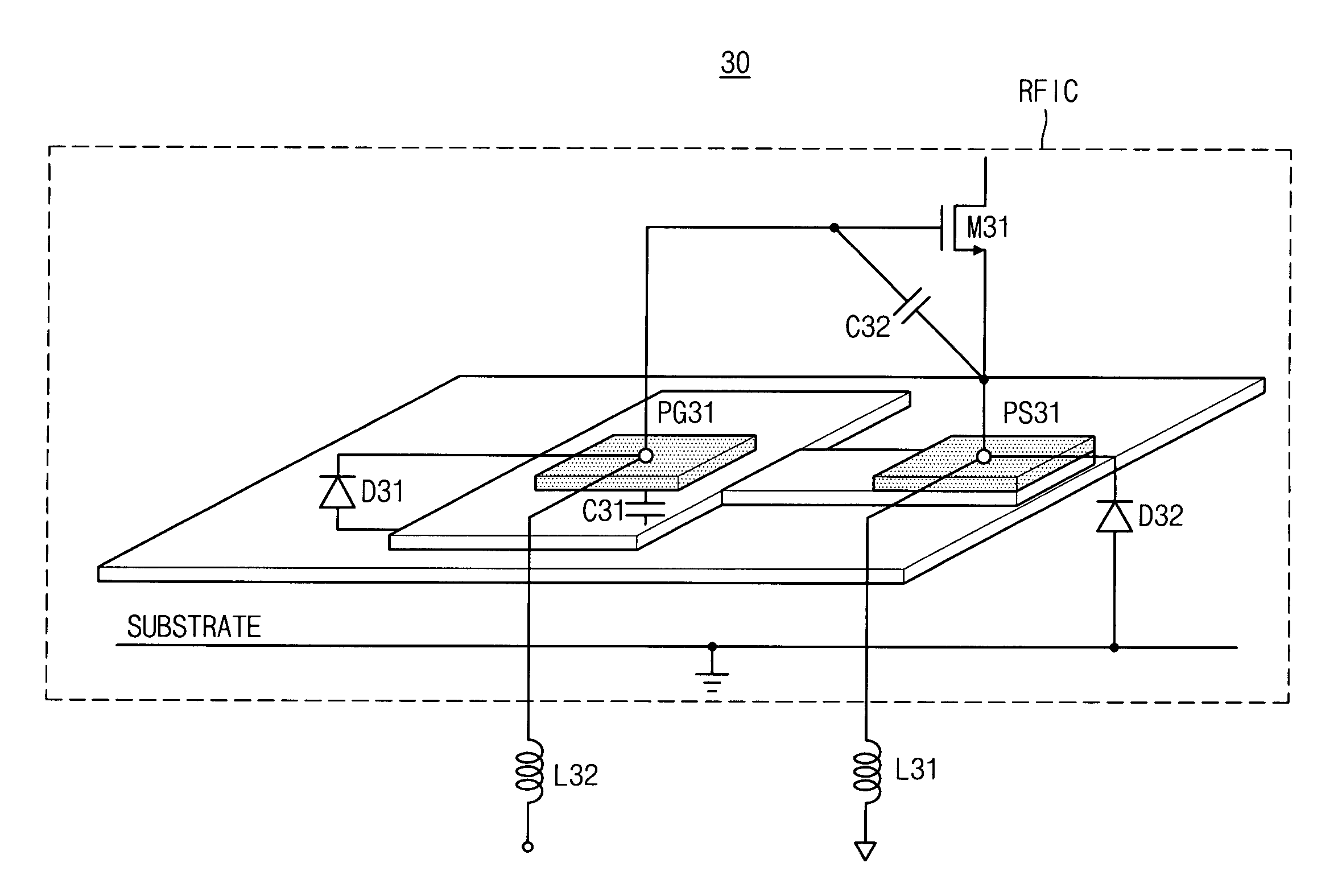
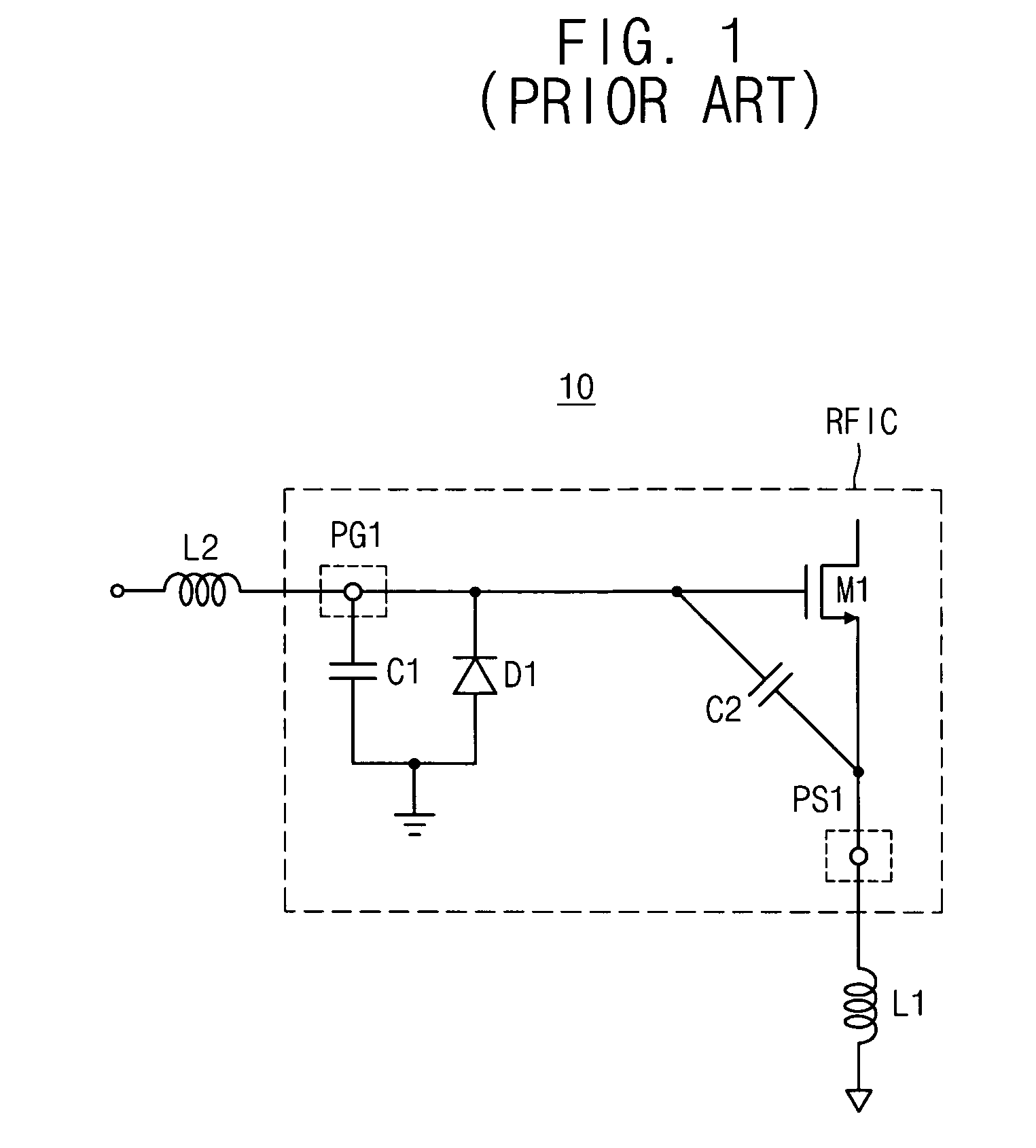
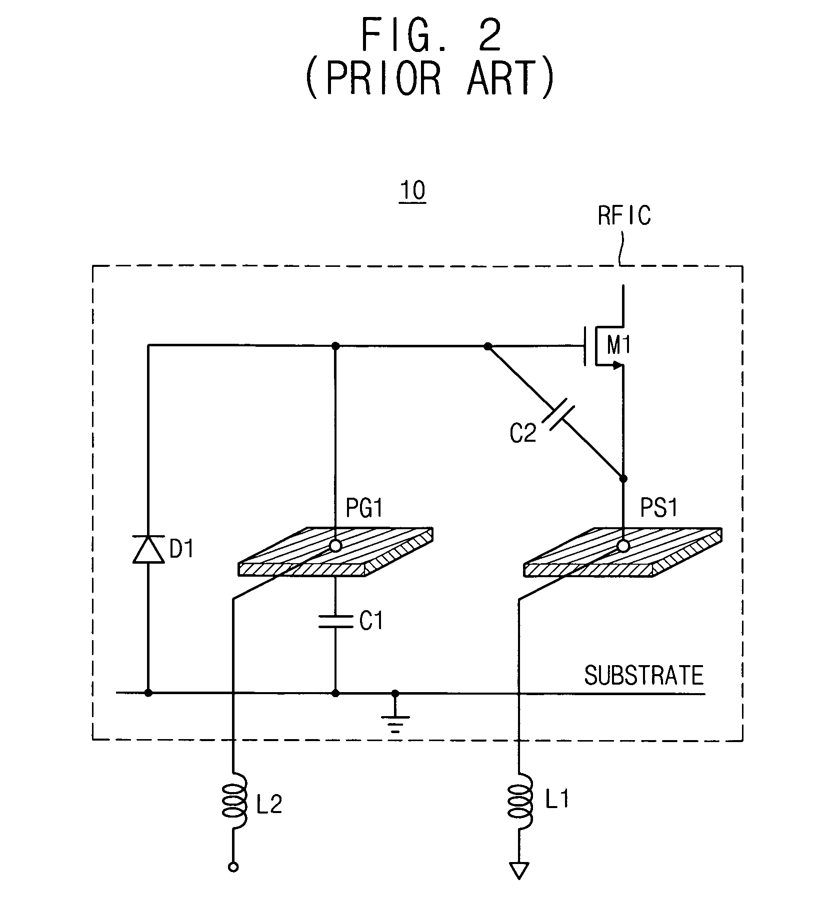
[0034]FIG. 3 shows an equivalent circuit diagram illustrating a receiving end of a low noise amplifier 30 according to an exemplary embodiment of the present invention...


PUM


Abstract

An input impedance matching circuit for a low noise amplifier includes a source pad, a gate pad, an input transistor, a source degeneration inductor and a matching capacitor. The gate pad receives an input signal and the input transistor amplifies the input signal transmitted from the gate pad. The source degeneration inductor electrically coupled to an external ground voltage is adapted for input impedance matching of the low noise amplifier. The source pad is coupled to a source electrode of the input transistor and the matching capacitor is formed between the gate pad and the source pad extending the source pad to be disposed under the gate pad. Accordingly, impedance matching of the low noise amplifier may be facilitated and the gain and noise figure of the low noise amplifier may be improved.

Description

CLAIM FOR PRIORITY[0001]This application claims priority under 35 USC § 119 to Korean Patent Application No. 2004-78161, filed on Oct. 1, 2004, the contents of which are herein incorporated by reference in its entirety.BACKGROUND OF THE INVENTION[0002]1. Field of the Invention[0003]The present invention relates to a receiving end of a low noise amplifier, and more particularly to a circuit for electrostatic discharge protection and input impedance matching of the low noise amplifier.[0004]2. Description of the Related Art[0005]Generally, a low noise amplifier having improved noise characteristics is used at a radio frequency (RF) receiver end to amplify a received RF signal. In addition, the low noise amplifier is used for impedance matching between internal elements of the low noise amplifier and an external circuit.[0006]A degeneration inductor is widely used for impedance matching of a low noise amplifier. However, when a degeneration inductor is used for impedance matching of a ...

Claims


Application Information

Patent Timeline
Patent Type & Authority Patents(United States)
IPC IPC(8): H03G3/12
CPCH03F1/26H03F1/523H03F1/565H03H7/38H03F2200/372H03F2200/444H03F2200/492H03F2200/294H03F1/56
Inventor KANG, SANG-HOON
Owner SAMSUNG ELECTRONICS CO LTD
Why Eureka
Try Eureka