Apparatus and method for producing single crystal, and silicon single crystal

a technology of single crystal and single crystal, applied in the direction of crystal growth process, polycrystalline material growth, crystal growth process, etc., can solve the problems of deterioration of electrical properties, isolation properties, difficult to set v/g values, etc., and achieve high pulling speed, defect-free region, and increase the vertical gradient at the solid-liquid interface neighborhood.

Active Publication Date: 2007-11-27
SUMCO CORP
View PDF5 Cites 8 Cited by
  • Summary
  • Abstract
  • Description
  • Claims
  • Application Information

AI Technical Summary

Benefits of technology

[0032]According to this invention, the silicon single crystal is grown while being pulled, while the silicon melt is applied with a cusp magnetic field the shape of neutral plane of which is symmetric with respect to the rotation axis of the silicon single crystal and is curved upward. Accordingly, in the region near the wall position of the crucible, vertical component of the magnetic field is generated and the silicon melt flow in the horizontal direction is controlled. Due to this, a low temperature region spreads out at the surface of the silicon melt, and a downward flow in the downward vertical direction is promoted. The upward flow of the silicon melt in the center portion of the crucible is enhanced, so that the degree of upward protrusion of the solid-liquid interface is increased, and at the solid-liquid interface neighborhood, thermal gradient in the vertical direction is increased. As a result, the pulling speed of the silicon single crystal is increased, and a silicon single crystal having a defect free region is produced with good efficiency.
[0037]By the curvature of magnetic field neutral plane, in the region near the wall position of the crucible, vertical component of the magnetic field is generated and the silicon melt flow in the horizontal direction is controlled, and the rising flow of the silicon melt in the center portion of the crucible is enhanced. However, in order to obtain a greater thermal gradient in the vertical direction near the solid-liquid interface, it is necessary to control the convection of the silicon melt in a more concrete manner. Therefore, in the invention, a rotation device which, when pulling the silicon single crystal, rotates the crucible at a rotation speed less than or equal to 3 min−1 is provided. The magnetic field generation unit generates the cusp magnetic field so that the vertical position of the magnetic field neutral plane is within the range of from 30 mm to 120 mm below the solid-liquid interface, and at the wall position of the crucible, the horizontal component of the magnetic flux density at the vertical position of the magnetic field neutral plane is within the range of from 0.02 T to 0.09 T. The pulling up device pulls the silicon single crystal while rotating it in a direction opposite to the rotation direction of the crucible at a rotation speed greater than or equal to 12 min−1. By doing this, the convection of the silicon melt is effectively controlled, and this is extremely appropriate for producing a silicon single crystal having a defect free region at good efficiency.
[0039]According to this invention, the silicon single crystal is pulled while making the shape of the solid-liquid interface upwardly protruding, with the height of its central portion exceeding 10 mm with respect to its peripheral portion. Accordingly, the thermal gradient in the vertical direction at the solid-liquid interface neighborhood is increased, and it is possible to pull a silicon single crystal at a high pulling speed.

Problems solved by technology

The L / DLs also cause a deterioration of the electrical properties, such as leak properties, the isolation properties.
However, since the allowable range for the V / G value capable of forming a defect free region is extremely narrow, it is extremely difficult to setting the V / G value to be the specified value throughout the entire plane of the silicon single crystal, and maintain the V / G value within the allowable range from starting to ending of pulling the silicon single crystal.
Furthermore, it is also difficult to obtain very large thermal gradient G in the vertical direction while pulling the silicon single crystal.
Therefore, increase of pulling speed of the silicon single crystal is restricted, thus being impossible to highly enhance the productivity of the silicon single crystal.
Furthermore, the narrow allowable range of the V / G value results in narrow allowable range of the pulling speed of the silicon single crystal.
By deviation of pulling speed from the allowable range, defects are generated partially in the silicon single crystal.

Method used


Image

  • Apparatus and method for producing single crystal, and silicon single crystal
  • Apparatus and method for producing single crystal, and silicon single crystal
  • Apparatus and method for producing single crystal, and silicon single crystal

Examples


Embodiment Construction

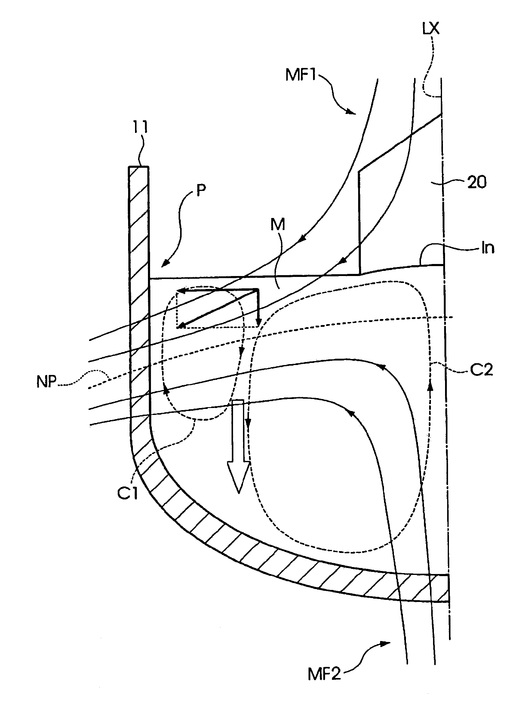
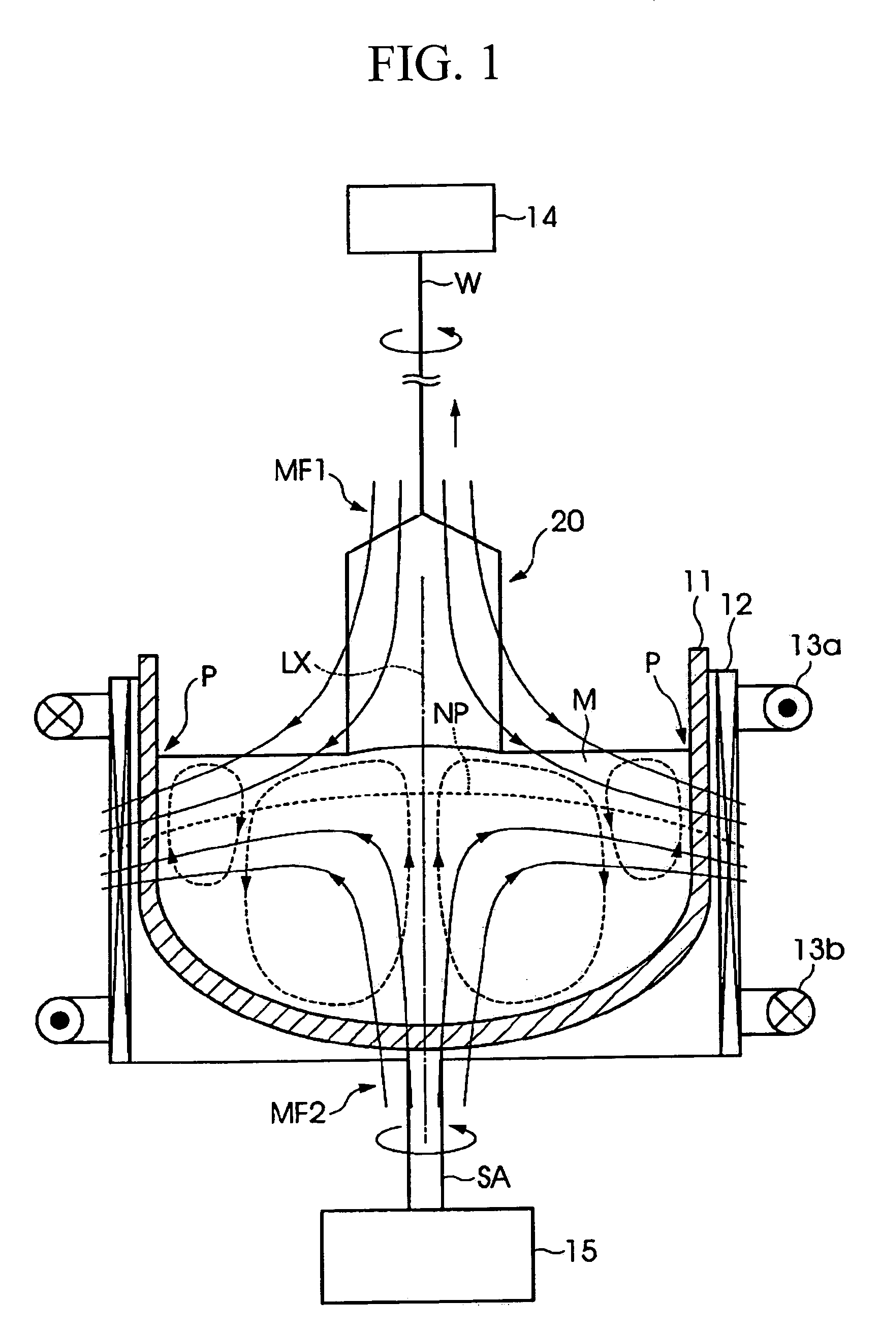
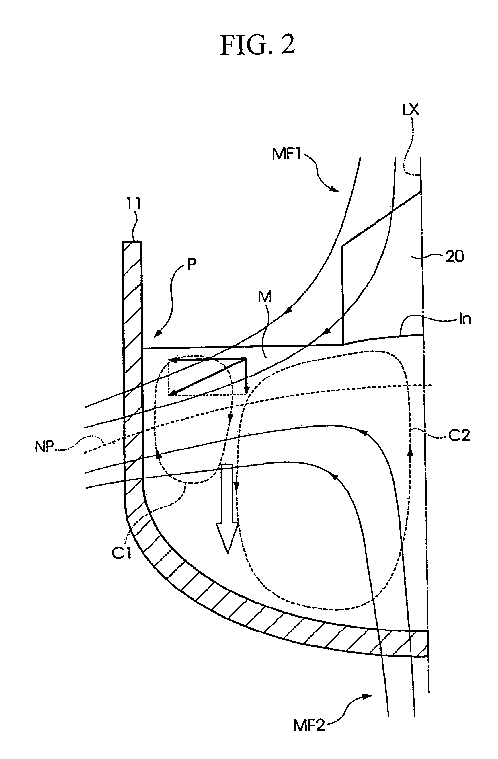
[0048]In the following, an apparatus and method for producing a single crystal, and a silicon single crystal, according to an embodiment of the invention will be explained in detail with reference to the drawings. FIG. 1 is a schematic view illustrating the overall structure of an apparatus for producing a single crystal in an embodiment of the invention. As shown in FIG. 1, the apparatus of this embodiment for producing a single crystal comprises a crucible 11, a heater 12, an upper coil 13a, a lower coil 13b, a pulling up device 14, and a rotation device 15. The crucible 11 is made from quartz or the like, and is filled with a polycrystalline silicon raw material. The heater 12 includes, for example, a high frequency wave heating device or a resistance heating device, and is arranged around the circumference of the crucible 11 and heats up the crucible 11, thus converting the polycrystalline silicon raw material to formsilicon melt M.

[0049]The upper coil 13a and the lower coil 13b...


PUM

PropertyMeasurementUnit
magnetic flux densityaaaaaaaaaa
heightaaaaaaaaaa
magnetic flux densityaaaaaaaaaa

Abstract

The invention provides an apparatus for producing a single crystal, and a method for producing a silicon single crystal using the same. An apparatus for producing a single crystal includes a heating device which heats polycrystalline silicon raw material held in a crucible to form silicon melt, and a pulling up device which grows a silicon single crystal while pulling it up from the silicon melt accompanied with rotation. By providing the apparatus with a magnetic field generation unit which applies to the silicon melt a cusp magnetic field a shape of neutral plane of which is symmetric around the rotation axis of the silicon single crystal and is curved in the upward direction, various conditions for producing a silicon single crystal having a defect free region is relaxed, and a silicon single crystal having a defect free region is produced at high efficiency.

Description

BACKGROUND OF THE INVENTION[0001]1. Field of the Invention[0002]The invention relates to an apparatus and a method for producing a silicon single crystal by crystal pulling by the Czochralski method (the CZ method), and to a silicon single crystal produced using the same method.[0003]Priority is claimed on Japanese Patent Application No. 2004-149251, filed 19 May, 2004, the content of which is incorporated herein by reference.[0004]2. Description of Related Art[0005]To produce a silicon single crystal, polycrystalline silicon raw material is held in a crucible and is heated by a heater to form silicon melt, and the silicon single crystal is grown while being pulled up from of the silicon melt by the CZ method. Silicon wafers are produced by slicing (cutting) the silicon single crystal produced by the above described method, and integrated circuits are formed upon the silicon wafers. For forming integrated circuits upon a silicon wafer, there are demands for a silicon wafer with high...

Claims


Application Information

Patent Timeline
Patent Type & Authority Patents(United States)
IPC IPC(8): C30B15/20C30B35/00C30B29/06C30B15/00C30B15/22C30B15/30
CPCC30B15/00C30B29/06C30B15/305Y10S117/917
Inventor FUKATSU, NORIHITOEGASHIRA, KAZUYUKIFU, SENRIN
Owner SUMCO CORP
Why Eureka
Try Eureka