Light emitting apparatus and method of manufacturing the same
a technology manufacturing method, which is applied in the direction of discharge tube luminescnet screen, discharge tube/lamp details, electric discharge lamps, etc., can solve the problems of reducing the reliability of light emitting apparatus, deterioration or discoloration of molding resin, and difficulty in making light emitting apparatus having sufficient reliability, etc., to improve the efficiency of wavelength conversion, improve workability, and minimize color unevenness with the direction
- Summary
- Abstract
- Description
- Claims
- Application Information
AI Technical Summary
Benefits of technology
Problems solved by technology
Method used
Image
Examples
embodiment 1
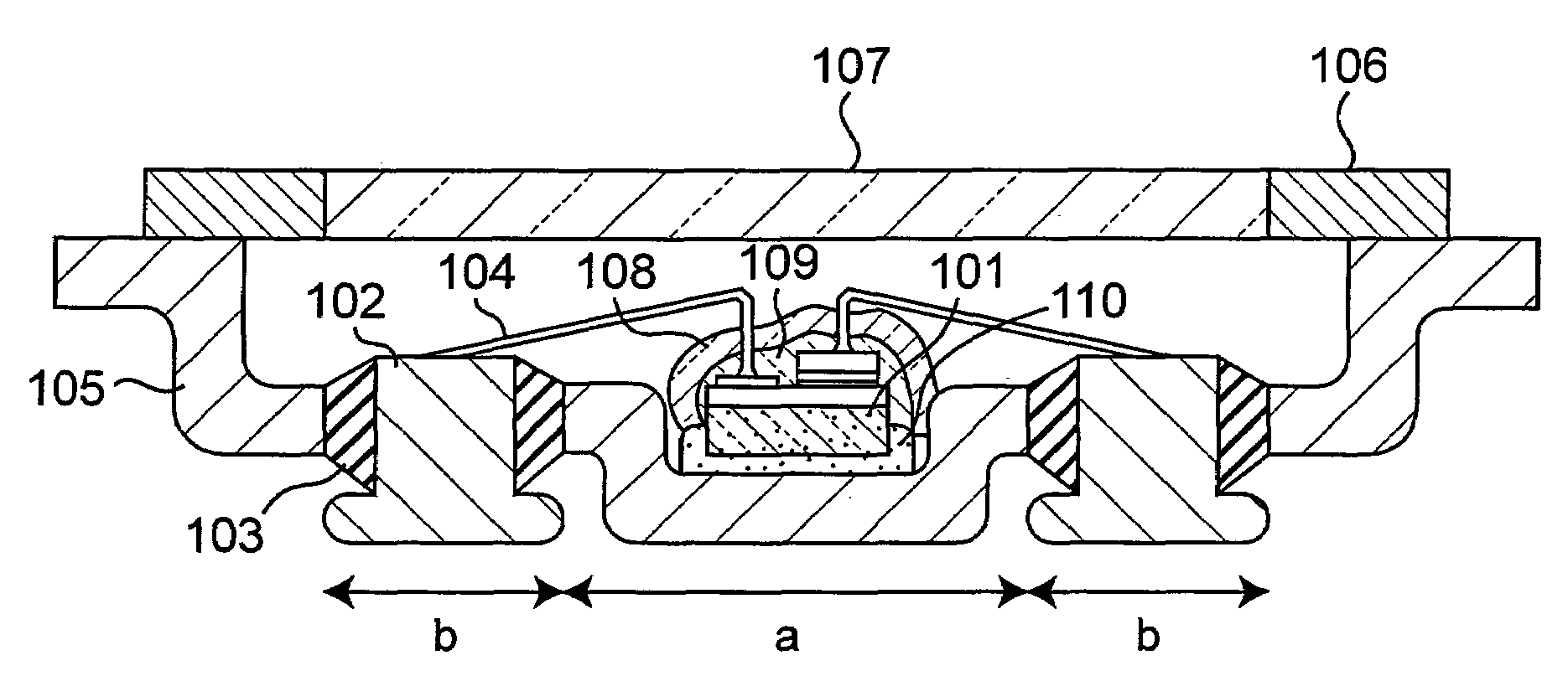
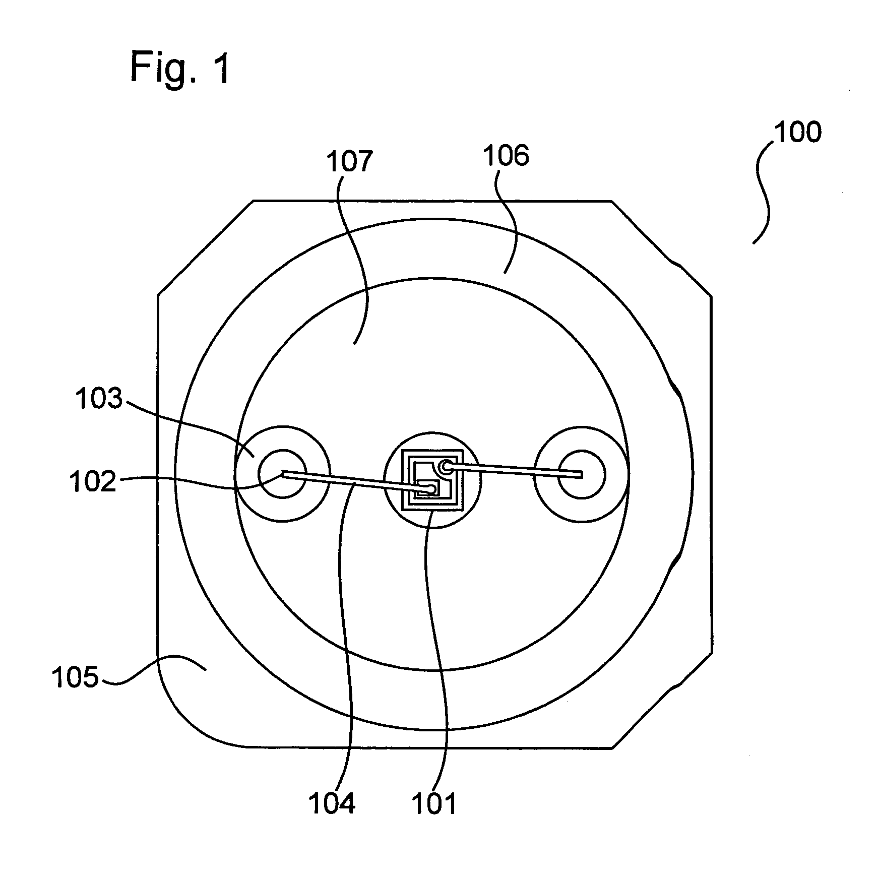
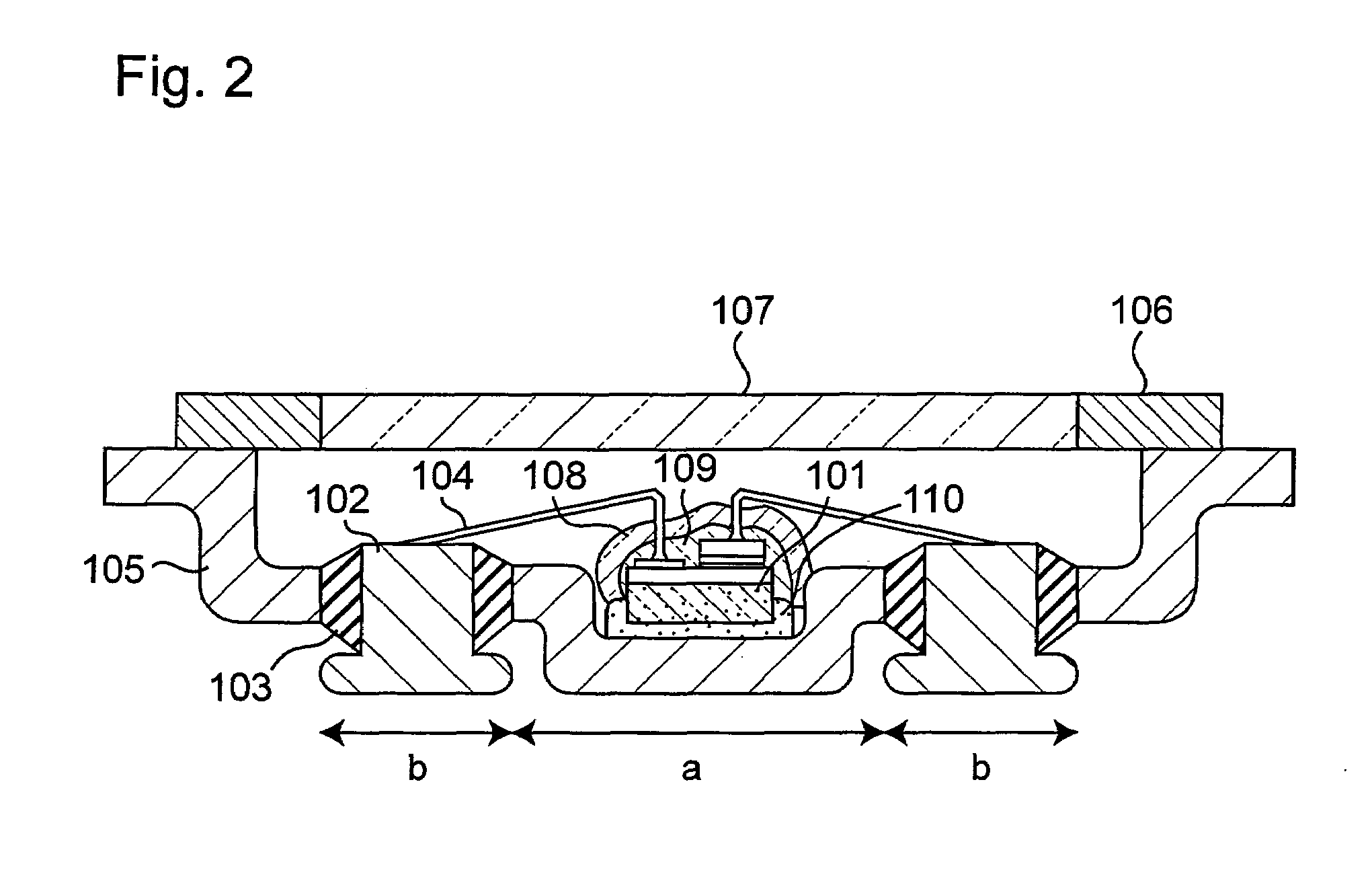
[0099]FIG. 1 and FIG. 2 are top view and sectional view, respectively, showing an example of a light emitting apparatus manufactured according to the method of the present invention.
[0100]In FIG. 1 and FIG. 2, an LED 101 that is a light emitting device is mounted in a metallic package 105. The package 105 has a recess “a” located at the center thereof. A base portion “b” that surrounds the recess “a” has two through holes penetrating in the direction of thickness, the through holes opposing each other across the recess “a”. Positive and negative lead electrodes 102 are inserted through the respective through holes via hard glass 103 that serves as an insulating member. The metal package 105 has a light transmitting window 107 and a lid 106 comprising a metal part provided on the principal surface thereof, so that the light emitting deice and other component are hermetically sealed together with nitrogen gas in the package, by welding the metallic part of the lid 106 and the contact ...
embodiment 2
[0234]FIG. 3 is a schematic sectional view showing another embodiment of the light emitting apparatus of the present invention.
[0235]This embodiment is an application of the present invention to an LED mounted on a resin package, unlike the first embodiment. FIG. 3 shows the structure of an LED package 114 that serves as supporting body whereon the LED 101 is mounted. Reference numeral 104 denotes an electrically conductive wire, 113 denotes a molding member, 111 denotes a coating layer provided on the LED chip, 112 denotes a coating layer provided on the supporting body and 110 denotes an adhesive layer. In this embodiment, the coating layers 111 and 112 are single layers of an oxide that consists mainly of SiO2 and contains fluorescent substance. The light emitting device 101 and the coating layers 111 and 112 are sealed with the molding resin 113, unlike in the first embodiment. The LED chip 101 is encased in the package 114, and is bonded onto one of external electrodes via sili...
embodiment 3
[0250]This embodiment is a method of spraying the coating solution in the form of spiral stream of mist that contains the fluorescent substance from above the light emitting device that is placed on the supporting body and is being heated. This method can be applied not only to the coating material of the present invention that is made of an inorganic material, but also to a coating material of the prior art that is made of an organic material.
[0251]FIG. 4 is a schematic diagram showing the process of spraying the coating solution to the light emitting device that is fastened onto the supporting body. This embodiment uses an apparatus that discharges the coating solution 203 and a gas (air in this embodiment) in a spiral stream from a nozzle 201. The apparatus has several gas vents disposed around the nozzle 201, while the gas discharged from these vents is directed toward the surface to be coated with a certain angle. As a result, as the gas is supplied through the vents that rotat...
PUM
 Abstract
Description
Claims
Application Information


