Semiconductor device and method for fabricating the same

a technology of semiconductor devices and semiconductor devices, applied in the direction of semiconductor devices, electrical equipment, transistors, etc., can solve the problems of increasing off leakage current, so as to reduce off leakage current and reduce power consumption of semiconductor devices

Active Publication Date: 2007-11-27
GK BRIDGE 1
View PDF2 Cites 117 Cited by
  • Summary
  • Abstract
  • Description
  • Claims
  • Application Information

AI Technical Summary

Benefits of technology

[0010]However, the conventional MISFET described above has a drawback in which power consumption of the semiconductor device is not reduced because of increased OFF leakage current in both cases of a p-MISFET and an n-MISFET.
[0011]It is therefore an object of the present invention to ensure reduction of power consumption in a MISFET, particularly a short-channel MISFET having a gate length of about 0.1 μm or less.
[0013]To reduce power consumption of a semiconductor device, OFF leakage current generally needs to be reduced by increasing a substrate dopant concentration under a gate electrode. However, in the case of a p-MISFET, for example, in the conventional MISFET which exhibits two peaks, i.e., a first peak in the dopant concentration distribution of the first n-type doped layer 9 as an upper layer and a second peak in the dopant concentration distribution of the second n-type doped layer 10 as a lower layer, and in which the dopant concentration at the second peak is higher than that at the first peak, if the dopant concentration of the first n-type doped layer 9 having the first peak in the dopant concentration distribution is increased so as to reduce OFF leakage current, the dopant concentration of the second n-type doped layer 10 having the second peak in the dopant concentration distribution also needs to be increased because the dopant concentration at the second peak needs to be higher than that at the first peak. This causes the dopant concentration near the junction between the second n-type doped layer 10 and the p-type source / drain doped regions 8 to increase, so that a greater electric field is generated upon an application of an operation voltage. As a result, OFF leakage current increases, and power consumption of a semiconductor device is not reduced. The same holds true for n-MISFETs. The OFF leakage current herein is current flowing between source and drain upon an application of an operation voltage across the source and the drain and no application of a voltage to the gate electrode.
[0014]The present invention has been accomplished based on the foregoing findings. Specifically, a semiconductor device according to the present invention includes: a gate electrode formed on a semiconductor substrate; source / drain regions formed in the semiconductor substrate at both sides of the gate electrode; a first doped layer of a conductivity type opposite to that of the source / drain regions, the first doped layer being formed in the semiconductor substrate and located under the gate electrode; and a second doped layer of the conductivity type opposite to that of the source / drain regions, the second doped layer being formed in the semiconductor substrate and located below the first doped layer. The first doped layer has a first peak in dopant concentration distribution in a depth direction. The first peak is located at a position shallower than a junction depth of the source / drain regions. The second doped layer has a second peak in dopant concentration distribution in a depth direction. The second peak is located at a position deeper than the first peak and shallower than the junction depth of the source / drain regions. A dopant concentration at the first peak is higher than that at the second peak. In this device, the first doped layer having the first peak in the dopant concentration distribution has a function of preventing punch-through between the extension regions and the second doped layer having the second peak in the dopant concentration distribution has a function of preventing punch-through between the source / drain regions.
[0015]In the semiconductor device of the present invention, the dopant concentration at the first peak in the dopant concentration distribution of the first doped layer formed in the semiconductor substrate under the gate electrode is higher than that at the second peak in the dopant concentration distribution of the second doped layer formed below the first doped layer, so that the following advantages are obtained. That is, even if the dopant concentration of the first doped layer having the first peak in the dopant concentration distribution is increased so as to reduce OFF leakage current, the dopant concentration of the second doped layer having the second peak in the dopant concentration distribution does not need to be increased because the dopant concentration at the second peak does not need to be higher than that at the first peak, unlike the conventional semiconductor device. Therefore, it is possible to keep the dopant concentration of the second doped layer low, so that the dopant concentration near the junction between the source / drain regions and the second doped layer of the conductivity type opposite to that of the source / drain regions is reduced, as compared to the conventional semiconductor device which has a threshold voltage approximately equal to that of the device of the present invention and in which the dopant concentration at the second peak is higher than that at the first peak. As a result, a smaller electric field is generated upon an application of an operation voltage, so that OFF leakage current decreases and, thereby, power consumption of the semiconductor device is reduced.
[0020]As described above, the present invention relates to a technique for fabricating a semiconductor device, and particularly to a technique which is effective when applied to a semiconductor device including a MISFET of a generation of a gate length of 0.1 μm or less. This technique ensures reduction of power consumption of the semiconductor device by reducing OFF leakage current.

Problems solved by technology

However, the conventional MISFET described above has a drawback in which power consumption of the semiconductor device is not reduced because of increased OFF leakage current in both cases of a p-MISFET and an n-MISFET.
As a result, OFF leakage current increases, and power consumption of a semiconductor device is not reduced.

Method used


Image

  • Semiconductor device and method for fabricating the same
  • Semiconductor device and method for fabricating the same
  • Semiconductor device and method for fabricating the same

Examples


embodiment 1

[0029]Hereinafter, a semiconductor device and a method for fabricating the device according to a first embodiment of the present invention will be described with reference to drawings.

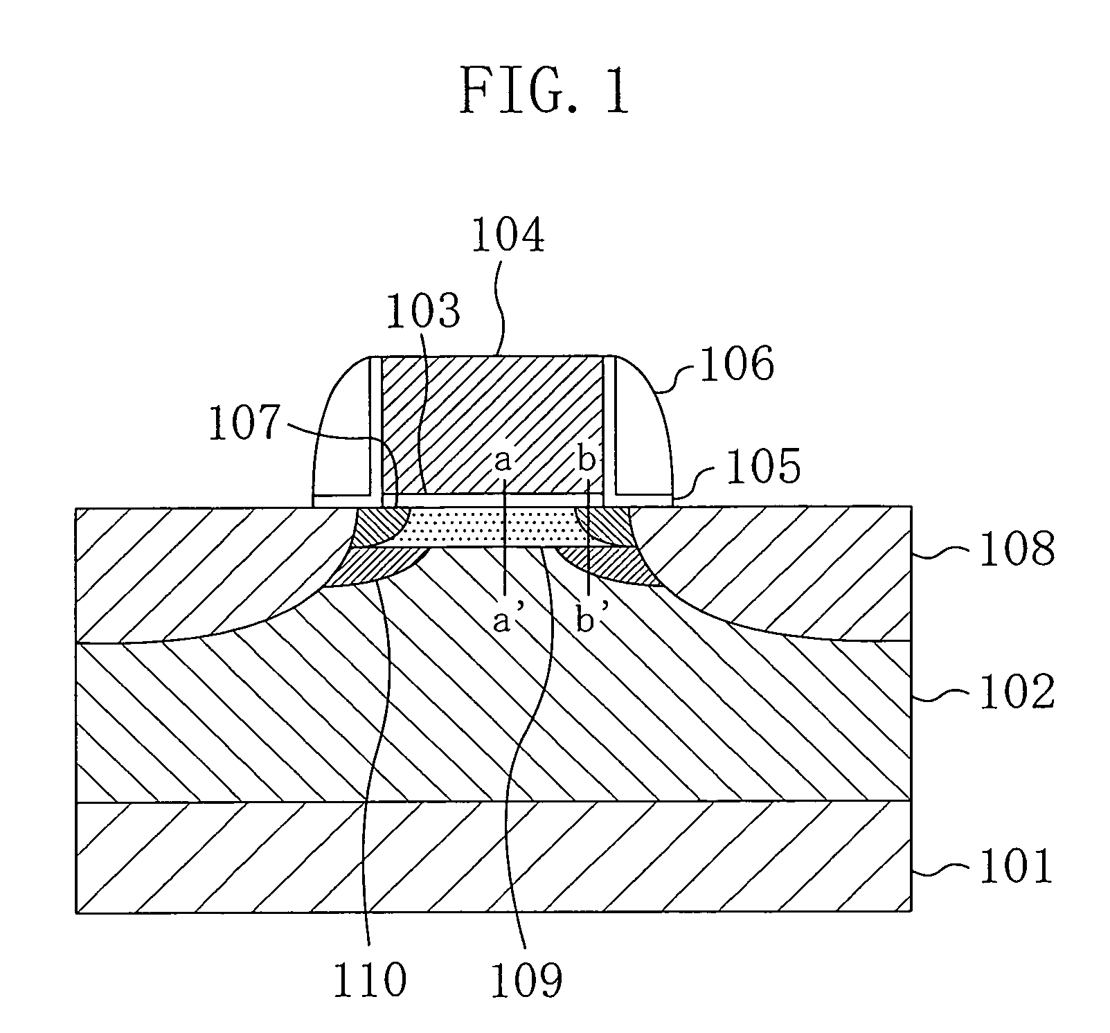
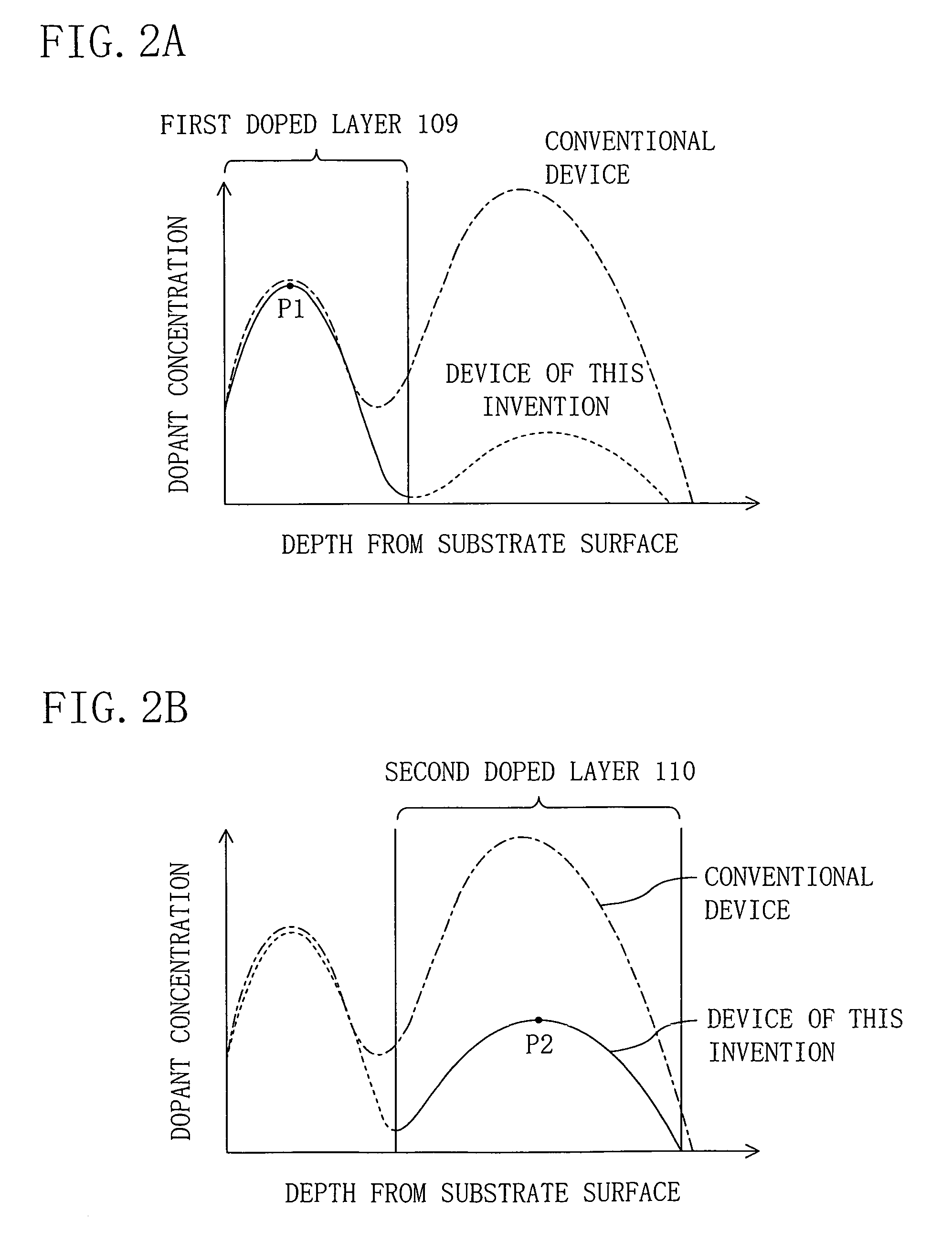
[0030]FIG. 1 is a cross-sectional view illustrating a semiconductor device according to the first embodiment, specifically a p-channel metal oxide semiconductor (p-MOS) device having a gate length of 0.1 μm or less.

[0031]As shown in FIG. 1, an n-well 102 is formed in a p-MISFET region (i.e., a region for forming a p-MISFET) of a substrate 101 made of, for example, p-type single crystalline silicon. A gate electrode 104 made of, for example, a p-type polycrystalline silicon film is formed over the p-MISFET region of the substrate 101 with a gate insulating film 103 interposed therebetween. Insulating sidewall spacers having a multilayer structure of; for example, a silicon oxide film 105 and a silicon nitride film 106 are formed on the sides of the gate electrode 104. P-type source / drain extension regio...

embodiment 2

[0052]Hereinafter, a semiconductor device and a method for fabricating the device according to a second embodiment of the present invention will be described with reference to drawings.

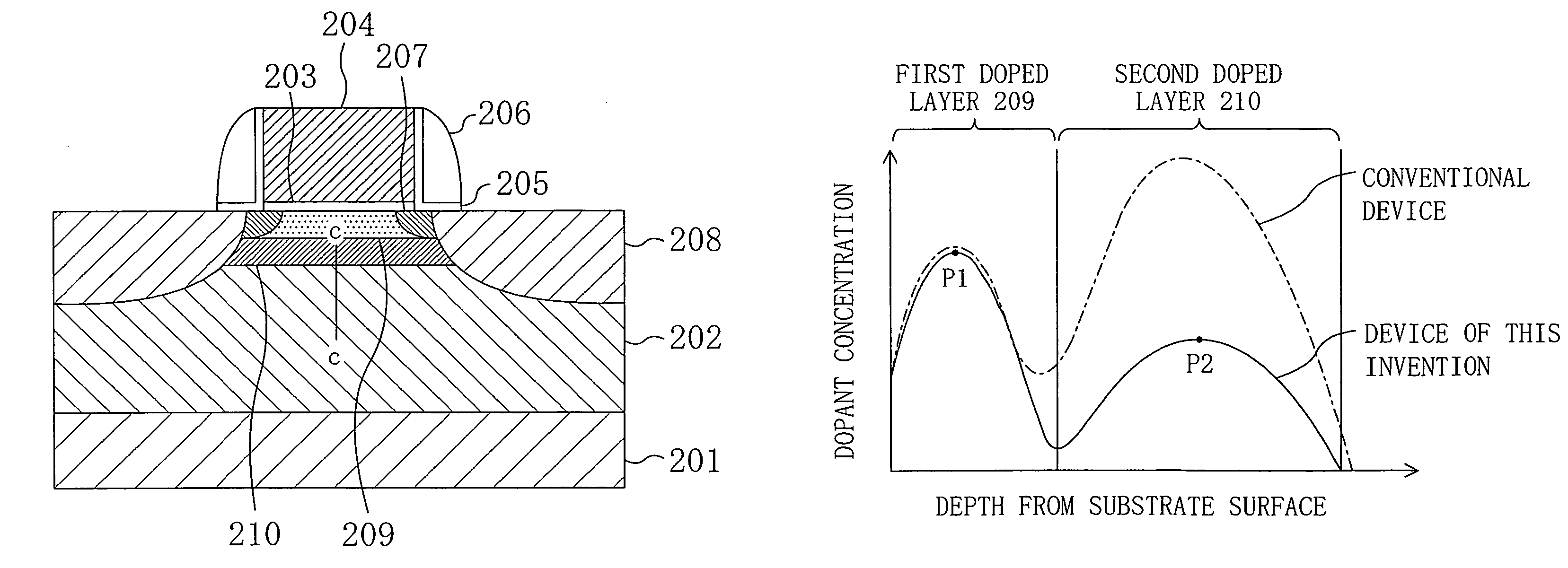
[0053]FIG. 5 is a cross-sectional view illustrating a semiconductor device according to the second embodiment, specifically a p-MOS device having a gate length of 0.1 μm or less.

[0054]As shown in FIG. 5, a well 202 of, for example, n-type is formed in a p-MISFET region of a substrate 201 made of, for example, p-type single crystalline silicon. A gate electrode 204 made of, for example, a p-type polycrystalline silicon film is formed over the p-MISFET region of the substrate 201 with a gate insulating film 203 interposed therebetween. Insulating sidewall spacers having a multilayer structure of, for example, a silicon oxide film 205 and a silicon nitride film 206 are formed on the sides of the gate electrode 204. Source / drain extension regions 207 of, for example, p-type are formed in a surface portion...


PUM


Abstract

A first doped layer of a conductivity type opposite to that of source / drain regions is formed in a semiconductor substrate under a gate electrode. A second doped layer of the conductivity type opposite to that of the source / drain regions is formed in the semiconductor substrate below the first doped layer. The first doped layer has a first peak in dopant concentration distribution in the depth direction. The first peak is located at a position shallower than the junction depth of the source / drain regions. The second doped layer has a second peak in dopant concentration distribution in the depth direction. The second peak is located at a position deeper than the first peak and shallower than the junction depth of the source / drain regions. The dopant concentration at the first peak is higher than that at the second peak.

Description

CROSS-REFERENCE TO RELATED APPLICATION[0001]The disclosure of Japanese Patent Application No. 2004-227688 filed on Aug. 4, 2004 including specification, drawings and claims is incorporated herein by reference in its entirety.BACKGROUND OF THE INVENTION[0002]The present invention relates to a technique for fabricating a semiconductor device, and particularly to a technique which is effective when applied to a semiconductor device including a metal insulator semiconductor field effect transistor (MISFET) of a generation of a gate length of 0.1 μm or less.[0003]As a MISFET in which a short-channel effect is suppressed, a MISFET having two peaks in substrate dopant concentration distribution under a gate electrode is disclosed in, for example, Japanese Unexamined Patent Publication (Kokai) No. 2002-198529.[0004]FIG. 8 is a cross-sectional view illustrating a conventional MISFET, specifically a conventional p-MISFET having a gate length of 0.1 μm or less. The conventional MISFET shown in...

Claims


Application Information

Patent Timeline
Patent Type & Authority Patents(United States)
IPC IPC(8): H01L29/76H01L29/94H01L31/062H01L21/336H01L21/8234H01L21/8238H01L27/088H01L27/092H01L29/78
CPCH01L29/0847H01L29/105H01L29/7833H01L29/6659H01L29/6656
Inventor HANDA, TAKATOKURIMOTO, KAZUMI
Owner GK BRIDGE 1
Why Eureka
Try Eureka