
Three-dimensional ferroelectric capacitor and method for manufacturing thereof as well as semiconductor memory device

Inactive Publication Date: 2007-12-04
SONY CORP
View PDF12 Cites 1 Cited by
  • Summary
  • Abstract
  • Description
  • Claims
  • Application Information

AI Technical Summary

Benefits of technology

[0024]A three-dimensional ferroelectric capacitor according to the present invention is a ferroelectric capacitor including a lower electrode formed on an inter-layer dielectric film which is formed on a substrate, a ferroelectric film formed on the lower electrode, and an upper electrode formed on the ferroelectric film, in which the above ferroelectric film has a plurality of protruding parts of three-dimensional shape formed on the surface thereof so as to expand the surface area of the ferroelectric film.
[0025]According to the three-dimensional ferroelectric capacitor of the present invention, since a plurality of protruding parts of three-dimensional shape are formed on the surface of the ferroelectric film so as to expand the surface area thereof, it is possible to compensate for a decrease in the amount of polarization of the ferroelectric film due to miniaturization of devices as well as to maintain the amount of polarization that is necessary for high integration without changing ferroelectric materials.

Problems solved by technology

However, the electric characteristics of these ferroelectric materials have been the cause of characteristic deterioration influenced by stress generated in an inter-layer dielectric film formed on the capacitor, compression stress occurring in a substrate, and tensile stress.
Of late, device elements tend to be miniaturized.
The former measure is, however, strongly dependant on the property of respective ferroelectrics, so that it is difficult to control the orientation and to realize the miniaturization of grains as designed.
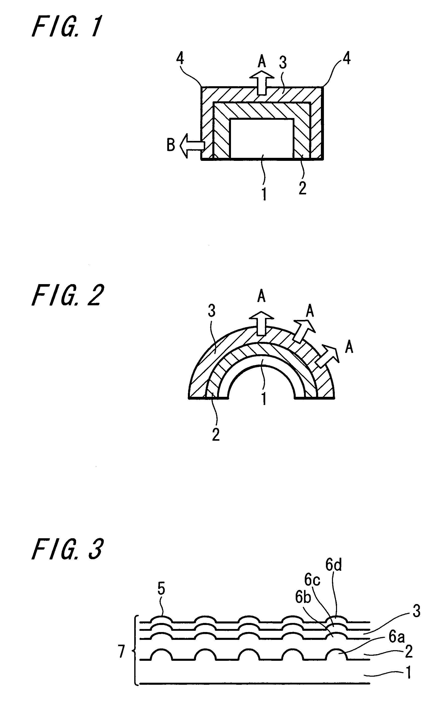
In addition, since the upper surface and sidewall surface each having a different orientation of crystallization collide with each other at a rectangular-shaped edge part 4, it is difficult to obtain continuous and homogeneous crystal, and a void tends to easily occur at this edge part, resulting in a crystallization defect.
However, there is a defect in the rectangular solid structure shown in FIG. 1.

Method used


Image

  • Three-dimensional ferroelectric capacitor and method for manufacturing thereof as well as semiconductor memory device
  • Three-dimensional ferroelectric capacitor and method for manufacturing thereof as well as semiconductor memory device
  • Three-dimensional ferroelectric capacitor and method for manufacturing thereof as well as semiconductor memory device

Examples


Embodiment Construction

[0039]Hereinafter, embodiments of the present invention will be explained with reference to the attached drawings.

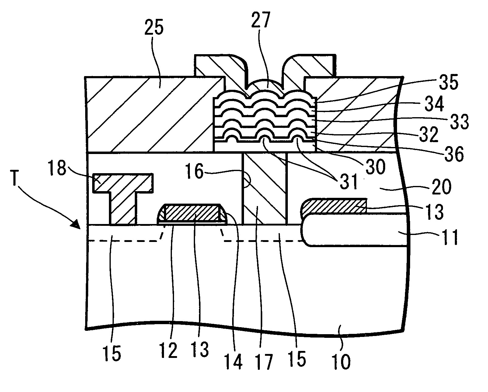
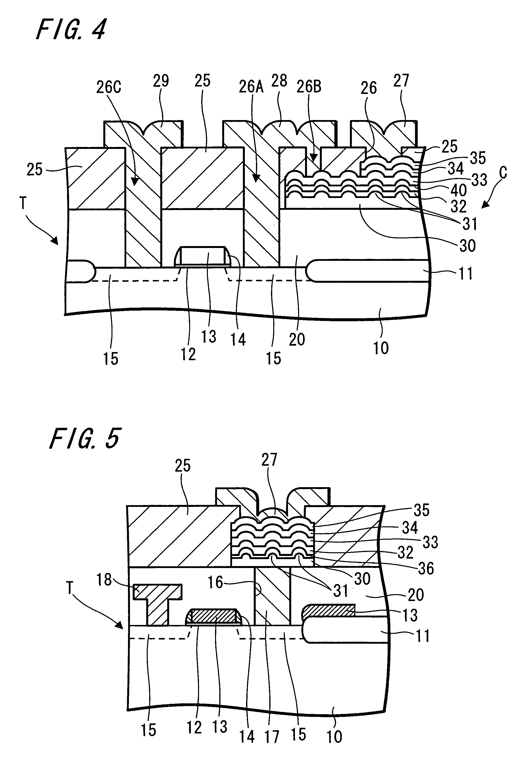
[0040]FIG. 1 is a conceptual diagram of a ferroelectric capacitor that has a three-dimensional structure. FIG. 2 is a conceptual diagram for explaining the three-dimensional structure of the ferroelectric capacitor that is an embodiment of the present invention. FIG. 3 is a partly cross-sectional diagram schematically showing an embodiment of the ferroelectric capacitor of the present invention, FIG. 4 is a partly cross-sectional diagram showing the structure of a planar-type semiconductor memory device using the ferroelectric capacitor that shows an embodiment of the present invention, and FIG. 5 is a partly cross-sectional diagram showing the structure of a stack-type semiconductor memory device using the ferroelectric capacitor that shows an embodiment of the present invention.

[0041]Hereinafter, embodiments of the present invention will be explained with reference to ...


PUM


Abstract

A ferroelectric capacitor is provided in which the surface area of a ferroelectric thin film is expanded to increase the amount of polarization. In the ferroelectric capacitor, hemi-spherical protruding parts 31 are formed with HSG-growth on the surface of a polycrystalline silicon film 30. On the polycrystalline silicon film 30 having the hemi-spherical protruding parts 31 are sequentially laminated an adhesive layer 32, lower electrode 33, ferroelectric film 34, and upper electrode 35. The ferroelectric film 34 is shaped to overlap the shape of hemi-spherical protruding parts 31 of the polycrystalline silicon film 30, and the surface area thereof is expanded.

Description

RELATED APPLICATION DATA[0001]The present application claims priority to Japanese Application(s) No(s). P2003-128184 filed May 6, 2003, which application(s) is / are incorporated herein by reference to the extent permitted by law.BACKGROUND OF THE INVENTION[0002]1. Field of the Invention[0003]The present invention relates to a three-dimensional ferroelectric capacitor that is suitable for being applied to a non-volatile semiconductor memory, for example, FeRAM (Ferroelectric Random Access Memory) and a method for manufacturing thereof as well as a semiconductor memory device using the three-dimensional ferroelectric capacitor.[0004]2. Description of the Related Art[0005]A ferroelectric type non-volatile semiconductor memory is composed of a dielectric capacitor section and selective transistor section, and its memory function is to make use of a spontaneous electric polarization phenomenon inherent in a ferroelectric material of the dielectric capacitor section to store information by...

Claims


Application Information

Patent Timeline
IPC IPC(8): H01L21/20H01L27/105H01L21/00H01L21/02H01L21/44H01L21/8242H01L21/8246H01L27/115
CPCH01L27/11502H01L28/55H01L27/11507H10B53/30H10B53/00H01L27/105
Inventor ISOBE, CHIHARUSAKAI, YOSHIO
Owner SONY CORP
Learn More