Cathode structure for inverted organic light emitting devices

a technology of organic light emitting devices and cathode structures, which is applied in the direction of discharge tubes/lamp details, discharge tubes luminescnet screens, electric discharge lamps, etc., can solve the problems of affecting the capability of electron injection on the interface of metal/organic, too high operating voltage to be applied in real display devices, and increase process control difficulty, etc., to achieve high activity, increase the capability of electron injection of inverted oled, and low work function

Inactive Publication Date: 2007-12-11
IND TECH RES INST
View PDF9 Cites 4 Cited by
  • Summary
  • Abstract
  • Description
  • Claims
  • Application Information

AI Technical Summary

Benefits of technology

[0009]It is the primary object of the present invention to provide a cathode structure for an inverted OLED, which includes an electron injection layer containing no metals of high activity and low work function and a cathode layer. The electron injection layer can increase the electron injection capability of the inverted OLED so as to improve the optoelectronic characteristics of the inverted OLED.
[0010]It is another object of the present invention to provide a cathode structure for an inverted OLED, which possesses the excellent electron injection capability without using metals of high activity and low work function so as to prevent the problem of deterioration and be more compatible to the current OLED manufacturing process, and thus enable the inverted OLED to be applied in an active-matrix organic light emitting display (AMOLED).

Problems solved by technology

However, the operating voltage is too high to be applied in real display devices.
However, in a common transistor, such as a-Si field effect transistor (FET) and poly-Si FET, the electric characteristics of p-channel transistor like carrier mobility are obviously inferior to those of n-channel transistor, and thus there is only n-channel transistor available for the a-Si FET.
However, such metals usually have high chemical activity and are easy to deteriorate, that increases the difficulty of process control while the OLED is mass-produced.
Besides, the different deposition sequence of metal and organic material will also affect the capability of electron injection on the interface of metal / organic.
However, the electron injection capability is not good enough, that cause the operating voltage of the OLED is still too high.
In addition, to use metal Mg for the bottom cathode will result in the problem of easy deterioration due to its high chemical activity so that such method will affect the device characteristics, causing some integration problems in the following processes for manufacturing organic light emitting displays.
However, the electron injection layer of the cathode of the foregoing OLED is formed by doping an organic material layer with metals of high activity and low work function as n-type dopants, that the above mentioned method still suffer the same difficulty of handling metals of high activity and low work function.
In addition, atoms of such metals, i.e. Li and Cs, are easily diffused in the organic material, which will affect the operating of device.
Moreover, it is still difficult to handle the metals with high chemical activity in the process for manufacturing organic light emitting display.

Method used


Image

  • Cathode structure for inverted organic light emitting devices
  • Cathode structure for inverted organic light emitting devices
  • Cathode structure for inverted organic light emitting devices

Examples


embodiment 1

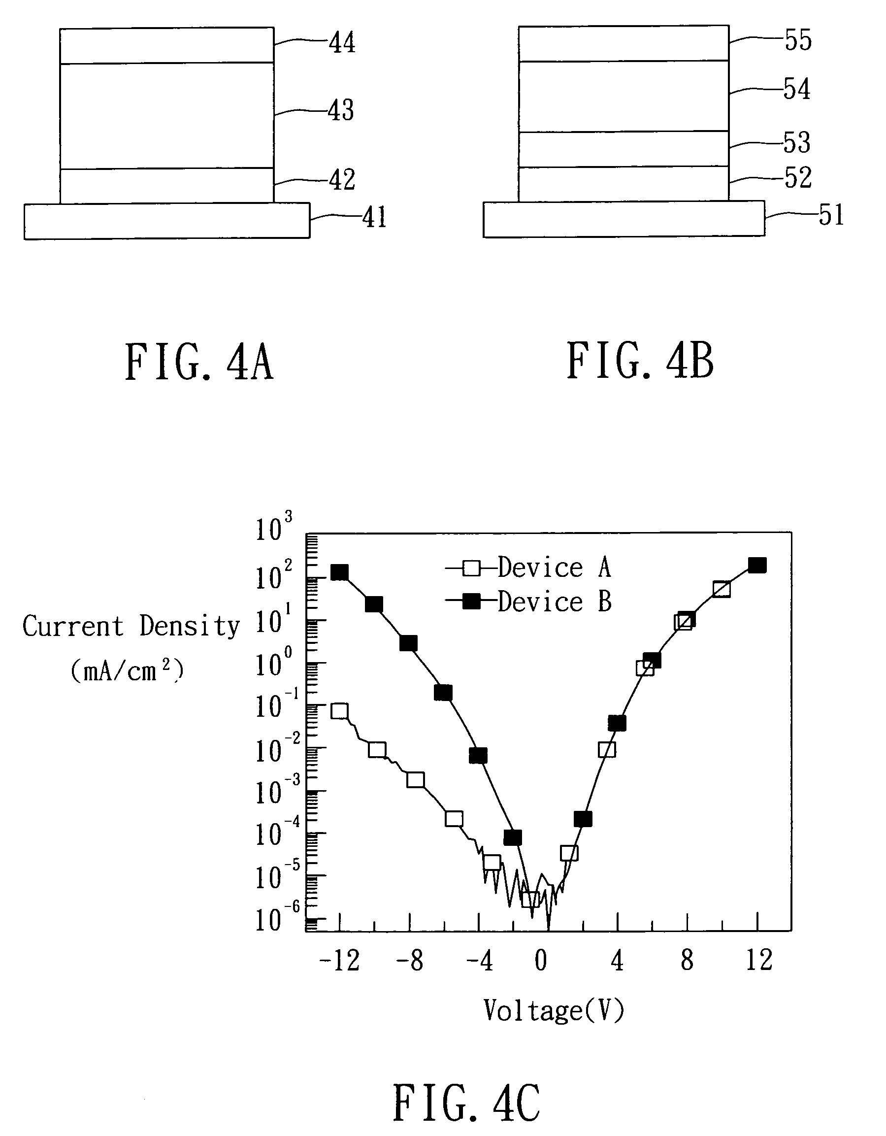
[0038]To illustrate that the electron injection layer of the present invention is capable of improving the electron injection capability of the inverted OLED having the cathode made of Ag, we use the bicathode electron / single carrier device for the comparison.

[0039]Please refer to FIG. 4A, Device A of the present embodiment comprises a substrate 41 made of glass, a bottom cathode layer 42 made of Ag with 80 nm in thickness, an organic electron transporting layer 43 made of Alq3 with 80 nm in thickness, and a top cathode layer 44 made of a stacked structure of LiF / Al with 0.5 nm and 100 nm in thickness respectively.

[0040]Please refer to FIG. 4B, Device B comprises a substrate 51 made of glass, a bottom cathode layer 52 made of Ag with 80 nm in thickness, an electron injection layer 53 made of Alq3 / LiF / Al with 0.2 nm, 0.2 nm and 0.3 nm in thickness respectively, an organic electron transporting layer 54 made of Alq3 with 80 nm in thickness, and a top cathode layer 55 made of LiF / Al wi...

embodiment 2

[0043]To illustrate that the electron injection layer of the present invention is capable of improving the electron injection capability of the inverted OLED having the cathode made of Al, we use the bicathode electron / single carrier device for the comparison.

[0044]Please refer to FIG. 5A, Device C of the present embodiment comprises a substrate 61 made of glass, a bottom cathode layer 62 made of Al with 80 nm in thickness, an organic electron transporting layer 63 made of Alq3 with 80 nm in thickness, and a top cathode layer 64 made of LiF / Al with 0.5 nm and 100 nm in thickness respectively.

[0045]Please refer to FIG. 5B, Device D comprises a substrate 71 made of glass, a bottom cathode layer 72 made of Al with 80 nm in thickness, an electron injection layer 73 made of Alq3 / LiF / Al with 0.2 nm, 0.2 nm and 0.3 nm in thickness respectively, an organic electron transporting layer 74 made of Alq3 with 80 nm in thickness, and a top cathode layer 75 made of LiF / Al with 0.5 nm and 100 nm in...

embodiment 3

[0048]To illustrate the influence of adding an electron injection layer according to the present invention on the electron injection capability of the inverted OLED having the cathode made of Ag, we use the devices described hereinafter for the comparison.

[0049]In this embodiment, the structure of Device E can refer to FIG. 2A, wherein the substrate 21 is a glass substrate, the cathode layer 22 is made of Ag with 80 nm in thickness, the organic structure layer 23 is a stacked structure consisting of a layer of Alq3 with 50 nm in thickness, a layer of α-NPD with 40 nm in thickness, and a layer of a mixture of F4-TCNQ and 2 wt. % m-MTDATA with 20 nm in thickness. Moreover, the anode layer 24 is made of Ag with 20 nm in thickness, on which a refractive index matched layer made of TeO2 with 30 nm in thickness is formed.

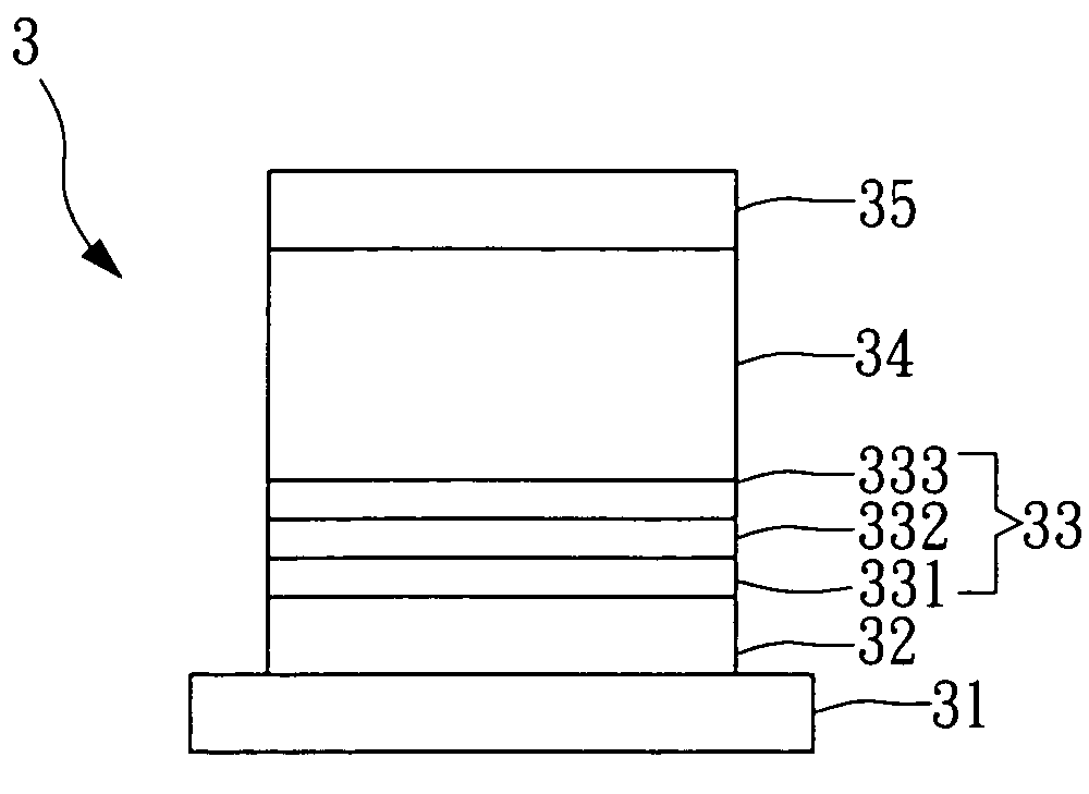
[0050]The structure of Device F can refer to FIG. 3, wherein the substrate 31 is a glass substrate, the cathode layer 32 is made of Ag with 80 nm in thickness, the electr...


PUM


Abstract

A cathode structure for inverted OLEDs is provided, which comprise a substrate, a conductive electrode layer, an organic material layer, a dielectric layer, and a metal layer. Wherein, the conductive electrode layer is disposed over the substrate, the organic structure layer is disposed over the conductive electrode layer, the dielectric layer is disposed over the organic material layer, and the metal layer is disposed over the dielectric layer. Such cathode structure can function without using the metals of low work function and high chemical activity so as to benefit the manufacturing of organic light emitting devices and displays, and provide a more stable working conditions.

Description

FIELD OF THE INVENTION[0001]The present invention relates to a cathode structure for inverted Organic Light Emitting Devices (OLED), in particular to a cathode structure for inverted OLEDs including an electron injection layer.BACKGROUND OF THE INVENTION[0002]For more than decades, researches focused on materials of organic conductive molecules and macromolecules were developing rapidly. By virtue of the maturity of organic conductor, insulator, and semiconductor materials, the application of such organic semiconductor materials in electronic devices and optoelectronic devices, such as organic light-emitting diodes, organic laser, organic memory, solar cells, thin film transistors (TFTs), and so on, have been gradually attracted their potential. Generally, the organic semiconductor-based optoelectronic devices possessing the characteristics of being fabricated as thin film device and by low temperature process can be used in various substrates and large size manufacturing process, t...

Claims


Application Information

Patent Timeline
Patent Type & Authority Patents(United States)
IPC IPC(8): H01J63/04
CPCH01L51/5092H01L51/0051H01L51/0059H10K85/611H10K85/631H10K50/171
Inventor YEH, YUNG HUIWU, CHUNG CHIHCHEN, CHIEH WEILIN, CHUN LIANGYANG, CHIH JEN
Owner IND TECH RES INST
Why Eureka
Try Eureka