Optical communication device, optical transmitter, optical transmitter-receiver, and optical transmission system

a communication device and optical transmitter technology, applied in the direction of electrical apparatus construction details, electrical instruments, support structure mounting, etc., can solve the problems of hard to meet the required specifications the standardized requirements are difficult to meet, so as to achieve the structural compactness of the optical transmitter and receiver, enhance cooling behavior, and increase the area of the circuit board

Active Publication Date: 2007-12-25
LUMENTUM JAPAN INC
View PDF11 Cites 3 Cited by
  • Summary
  • Abstract
  • Description
  • Claims
  • Application Information

AI Technical Summary

Benefits of technology

[0013]In order to attain the objects, a printed circuit board to mount components thereto is split into several parts and the respective parts are fixed to the housing in accordance with the dimensional specifications of the optical transmitter-receiver, which parts are interconnected to one another through connectors and so forth. The height of the housing is made lower by defining the fixing location of the respective components on the split parts in accordance with the height thereof. Due attention is paid when the split parts are overlapped such that they make no contact with one another. This enlarges the area of the circuit board to mount the components thereon with the realization of the structural compactness of the optical transmitter-receiver. Further, because the packaging side of the circuit board is selected in an arbitrary manner in accordance with the cooling direction of the respective ICs, it allows such direction to be oriented to the side of the heat sinks. This enhances cooling behavior. Moreover, when deteriorated parts are found, only the split part with such parts mounted is repaired or replaced with another so as to improve productivity and reduce production cost.

Problems solved by technology

In the above prior packaging method, one sheet of printed circuit board is adopted so that the dimension of the board depends on the size and quantity of the respective components, which makes it hard to meet the standardized requirements especially in the case of a high-density packaging process.
Such large height of the housing 20 makes it hard to meet the required specifications of the optical transmitter-receiver.
Another issue related with the packaging side of the circuit board that is controlled by the height of the respective components is concerned with the components requiring cooling process, especially, an IC whose cooling side is normally controlled by the packaging side of the circuit board.

Method used


Image

  • Optical communication device, optical transmitter, optical transmitter-receiver, and optical transmission system
  • Optical communication device, optical transmitter, optical transmitter-receiver, and optical transmission system
  • Optical communication device, optical transmitter, optical transmitter-receiver, and optical transmission system

Examples


first embodiment

[0029]FIG. 4 is a partly sectional side view of one example of the optical transmitter-receiver according to the invention, and FIG. 5 is an exemplary view of the disposition of the components of the optical transmitter-receiver according to the invention. FIG. 4 shows the optical transmitter and receiver arranged substantially in the same manner and the cross sectional view thereof taken along the line A1-A2 or B1-B2.

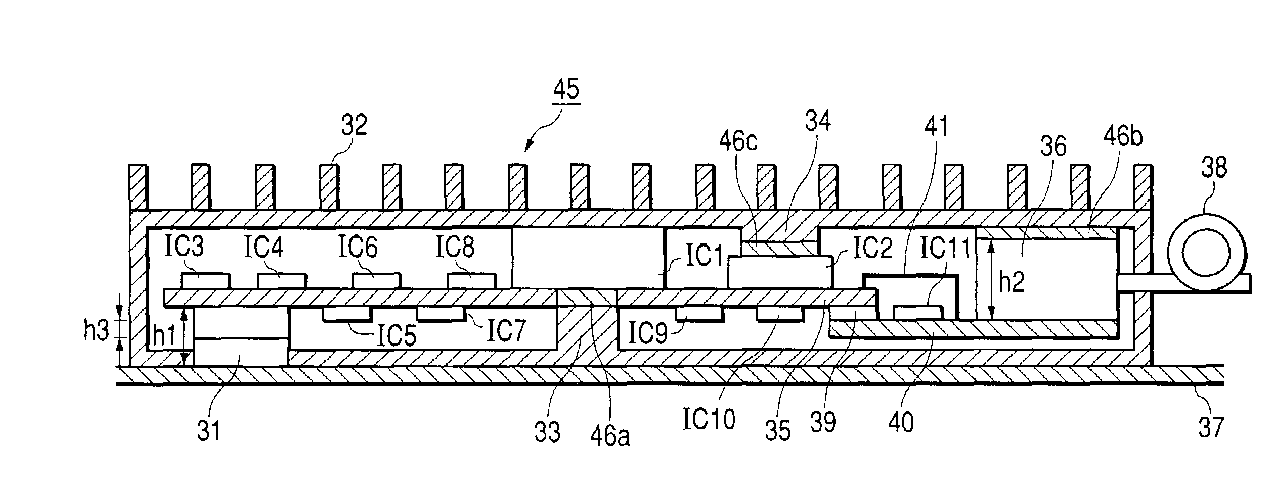
[0030]In this embodiment, a printed circuit board contained in a housing 45 provided with heat sinks 32 is divided into circuit boards 35 and 40. An electric connector 31 with the height of h1 is connected between a mother board 37 and the printed circuit board 35. ICs 1 to 10 are mounted on the printed circuit board 35 while an IC11 and an optical device module 36 are mounted on the printed circuit board 40. Among the components mounted on the printed circuit boards 35 and 40, it is assumed that the highest component of all is the optical device module 36. The printed...

second embodiment

[0039]FIG. 6 is an exemplary view of the disposition of the components of the optical transmitter-receiver according to the invention. As shown in the figure, the light emitting device driving circuit 3 is consolidated into the light emitting device module 4 so as to turn into a driving circuit combined light emitting device module 48, and the amplification circuit 13 is consolidated into the light receiving device module so as to turn into an amplification circuit combined light receiving device module 12. As mentioned above, the light emitting device driving circuit 3 may be consolidated into the clock multiply and data multiplexing circuit 54, and the amplification circuit 13 may be consolidated into the discrimination and isolation circuit 55.

third embodiment

[0040]FIG. 7 is an exemplary view of the disposition of the components of the optical transmitter-receiver according to the invention. As shown in the figure, the printed circuit board is split into circuit boards 40a and 40b, in which board 40a there are mounted a light emitting device module 4 and a light emitting device driving circuit 3 and in which board 40b there are mounted a light receiving device module 12 and an amplification circuit 13. In this case, the fixing position of the respective circuit boards is set according to the size of the respective components, which gives larger latitude in the layout design of the circuit board. When deteriorated parts or defects are found, only the circuit board with such parts mounted is removed for repair or replacement, resulting in improvement of productivity.


PUM


Abstract

The printed circuit board with the respective components of the optical transmitter-receiver mounted thereon is split into several parts, the fixing position of which respective parts with regard to the housing is set according to the standardized size of the respective components and which respective parts are interconnected through an electric connector and so forth, which makes the height of the transmitter-receiver lower. The split circuit boards are overlapped such that they make no contact with one another so as to enlarge the area of the circuit boards or practically increase the packaging area of the respective components, which realizes the structural compactness of the optical transmitter-receiver. The packaging side of the respective components is selected in an arbitrary manner according to the cooling direction of the respective ICs, which allows such direction to be oriented to the side of the heat sinks so as to enhance cooling behavior. When deteriorated parts are found, only the circuit board with such parts mounted is removed for repair or replacement, resulting in improving productivity and reducing production cost.

Description

FIELD OF THE INVENTION[0001]The present invention relates to an optical communication device such as an optical transmitter and / or an optical receiver to be used for an optical communication system and an optical transmission system, in more details, pertaining to an optical transmitter-receiver technology to realize the compactness of the components thereof and a lower production cost thereof by implementing compactness, reduction in height, expanding the operating temperature range thereof as well as improving productivity thereof.PRIOR ART[0002]The optical transmitter of the optical fiber communication converts an input electrical signal into an optical signal so as to feed the latter to an optical fiber. The optical receiver receives the optical signal transmitted through the optical fiber so as to reproduce the initial electrical signal. The handling of a higher speed signal exceeding a GHz-scaled frequency complicates the processing of the electrical signal on the printed circ...

Claims


Application Information

Patent Timeline
Patent Type & Authority Patents(United States)
IPC IPC(8): H04B10/00H05K7/00H05K7/20H01L31/02H01S5/022H05K1/14H05K7/14
CPCH04B10/503H05K1/141
Inventor AKASHI, MITSUOSAITOH, HIRONORIGOTO, FUMITOSHIKANKIPATI, RAJUNAKAGAWA, HIROFUMI
Owner LUMENTUM JAPAN INC
Why Eureka
Try Eureka