
Semiconductor laser light source device and optical pickup device

a laser light source and semiconductor technology, applied in semiconductor lasers, optical beam sources, instruments, etc., can solve the problems of increased manufacturing costs, inability to provide another function such as chromatic aberration correction, and loss of light caused by diffractive ring-shaped zonal structure, etc., to achieve high precision and without lowering the transmittance of lens materials

Inactive Publication Date: 2008-01-08
KONICA MINOLTA OPTO
View PDF12 Cites 2 Cited by
  • Summary
  • Abstract
  • Description
  • Claims
  • Application Information

AI Technical Summary

Benefits of technology

"The invention relates to a semiconductor laser light source device that improves stability and efficiency of a laser beam, even in a recording method. The device includes a semiconductor laser oscillator and a lens made of light-transparent material with microparticles dispersed in plastic resin. By adjusting the state of the microparticles, the temperature coefficient of the refractive index can be controlled, resulting in desired image forming characteristics and temperature fluctuations of the laser beam can be controlled, keeping the image forming position at the desired state."

Problems solved by technology

However, in the semiconductor laser module stated above, it is necessary to form, on the light converging lens, a diffractive ring-shaped zonal structure for temperature compensation, which requires high technologies for making of the light converging lens, and a loss of light caused by the diffractive ring-shaped zonal structure cannot be avoided.
Further, when the diffractive ring-shaped zonal structure for temperature compensation is formed on the light converging lens, it is difficult to provide another function such as correction of chromatic aberration to the diffractive ring-shaped zonal structure of this kind.
In the semiconductor laser module, when the flat sheet lens equipped thereon with the diffractive ring-shaped zonal structure is provided separately from the light converging lens, the manufacturing cost is raised by an increase of the number of parts, and a loss of an amount of light caused by the flat sheet lens turns out to be reckoned with.

Method used


Image

  • Semiconductor laser light source device and optical pickup device
  • Semiconductor laser light source device and optical pickup device
  • Semiconductor laser light source device and optical pickup device

Examples


first embodiment

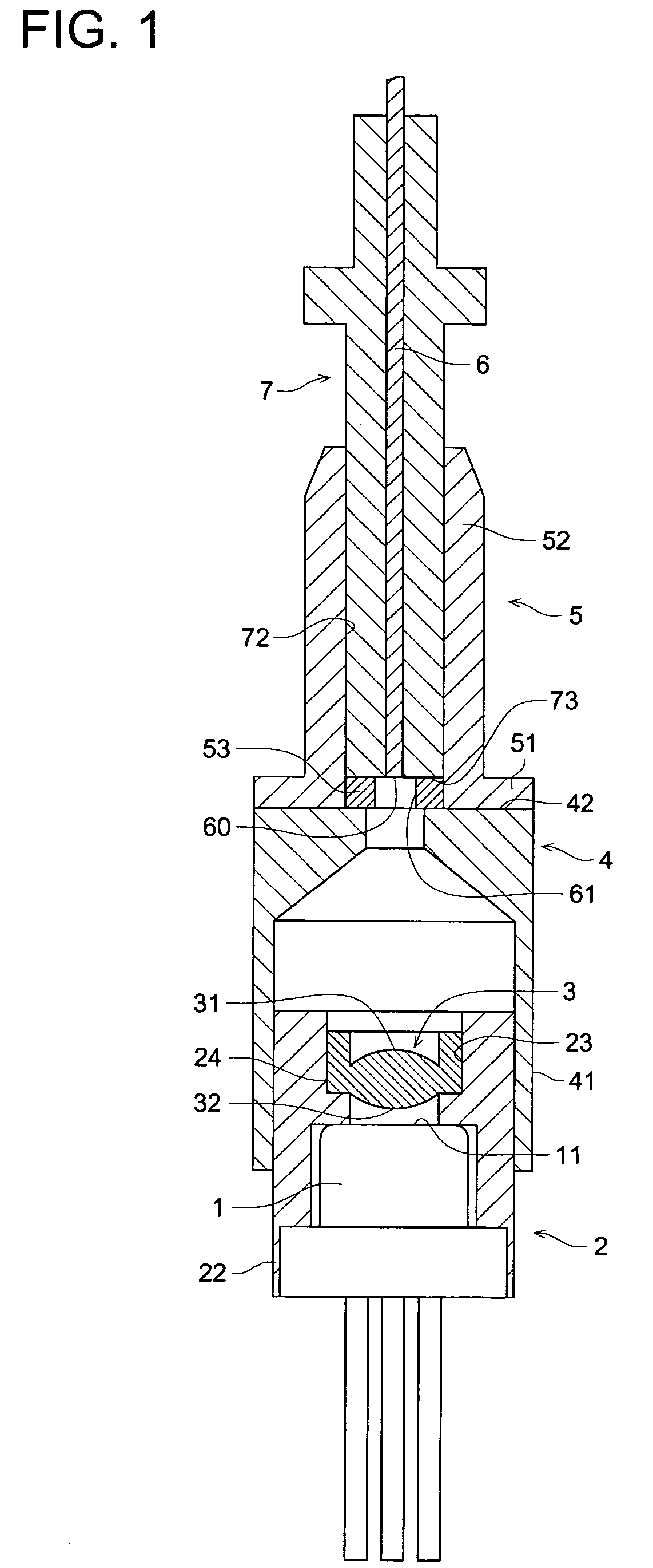
[0033]FIG. 1 shows a semiconductor laser module in which the semiconductor laser light source device related to the First Embodiment is incorporated. Semiconductor laser oscillator 1 is inserted into the hollow portion at the rear end portion of cylinder-shaped lens holder 2 through its opening, and is fixed through welding and others. On the other hand, in front of light-emitting portion 11 of semiconductor laser oscillator 1, light-converging lens 3 is inserted into the hollow portion at the front end portion of the lens holder 2 through its opening, and is fixed on the inner circumferential surface 23 of the hollow portion by adhesives. On outer circumferential surface 22 of the lens holder 2, there is fitted connecting cylindrical portion 41 of connecting holder 4.

[0034]To this connecting holder 4, there is connected ferrule holder 5 that holds optical fiber 6 through ferrule 7. Due to this, end portion of incidence 60 of the optical fiber 6 is fixed on the semiconductor laser o...

second embodiment

[0188]A semiconductor laser light source device relating to Second Embodiment is a variation of the device in the First Embodiment, and the structure in appearance of the semiconductor laser light source device is substantially the same as that of the device in the First Embodiment. However, in the Second Embodiment, semiconductor laser oscillator 1 is not cooled by force, and therefore, a wavelength of a laser beam emitted from the semiconductor laser oscillator 1 is shifted to the longer wavelength side as an ambient temperature rises.

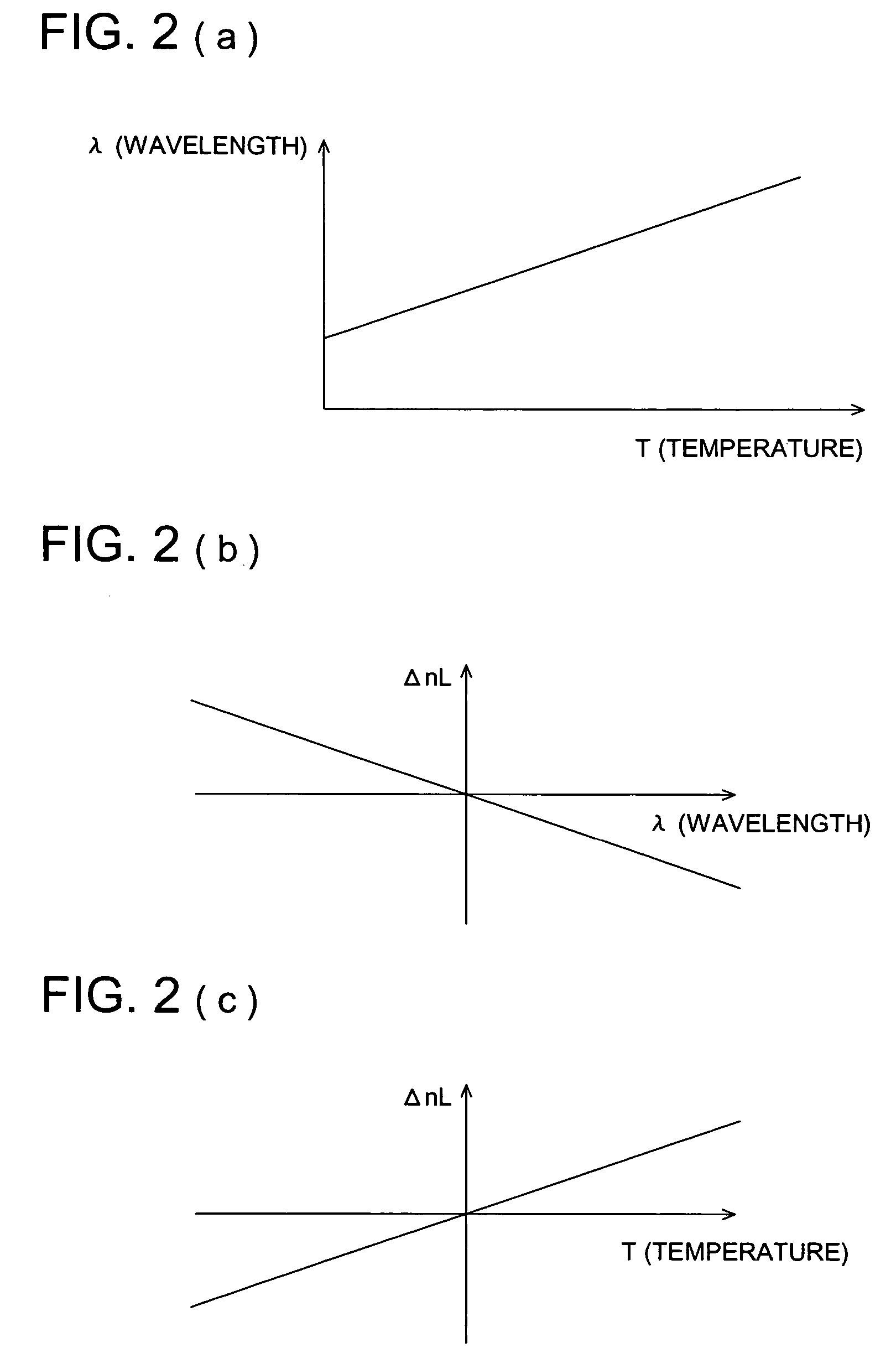
[0189]FIG. 2(a) shows an example of temperature-dependency of an oscillation wavelength of the semiconductor laser oscillator 1. As is shown, the oscillation wavelength is shifted to the longer wavelength side as a temperature rises. FIG. 2(b) shows apparent change ΔnL of the refractive index in the case where a wavelength of a laser beam entering light converging lens 3 is fluctuated. Further, FIG. 2(c) shows change ΔnT of the refractive index resul...

third embodiment

[0190]A semiconductor laser light source device relating to Third Embodiment is a variation of the device in the First Embodiment or the Second Embodiment. However, on the device of the Third Embodiment, an optical path difference providing structure including any one of a diffractive structure that generates an image-forming effect by utilizing a diffraction phenomenon, a phase difference providing structure for generating a certain light-converging effect by a phase difference and a multi-level structure that shifts plural partial surfaces obtained by dividing an optical surface into ring-shaped zonal state in the optical axis direction by a microscopic amount.

[0191]FIG. 3 is a plane view of light converging lens 103 wherein ring-shaped zones 135 are formed on the surface of optical surface 31 on one side (however, the ring-shaped zones 135 are shown in exaggeration in FIG. 3). When the ring-shaped zones 135 of this kind have a diffractive effect, the surface of each ring-shaped z...


PUM

PropertyMeasurementUnit
diametersaaaaaaaaaa
diameteraaaaaaaaaa
wavelength zoneaaaaaaaaaa

Abstract

An semiconductor laser light source apparatus includes: a semiconductor laser oscillator for emitting a laser beam; and a lens for transmitting the laser beam emitted by the semiconductor laser oscillator, wherein the lens comprises a light transparent material in which microparticles are dispersed into a plastic resin and have a size of the transmitting laser beam wavelength or below.

Description

BACKGROUND OF THE INVENTION[0001]The present invention relates to a semiconductor laser light source device, and in particular, to a semiconductor laser light source device that is preferably incorporated in a semiconductor laser module that is used for optical communication or optical measurement and conducts optical coupling between a laser beam and an optical fiber.[0002]As a semiconductor laser module, there exists one that converges a laser beam emitted from a semiconductor laser light source through and thereby forms images on an end of incidence of a fiber. There is in existence one (Patent Document 1) wherein, in the semiconductor laser module of this kind, a shift of focus caused by changes of oscillation wavelength of a semiconductor laser oscillator resulted from temperature changes and a shift of focus caused by changes of refractive index resulted from temperature changes of the light converging lens cancel each other, by forming a diffractive ring-shaped zonal structur...

Claims


Application Information

Patent Timeline
Patent Type & Authority Patents(United States)
IPC IPC(8): G11B7/00G02B6/42G11B7/125G11B7/127G11B7/135G11B7/1372H01S3/08H01S5/022
CPCG11B7/127G11B7/1372
Inventor ATARASHI, YUICHI
Owner KONICA MINOLTA OPTO
Learn More