

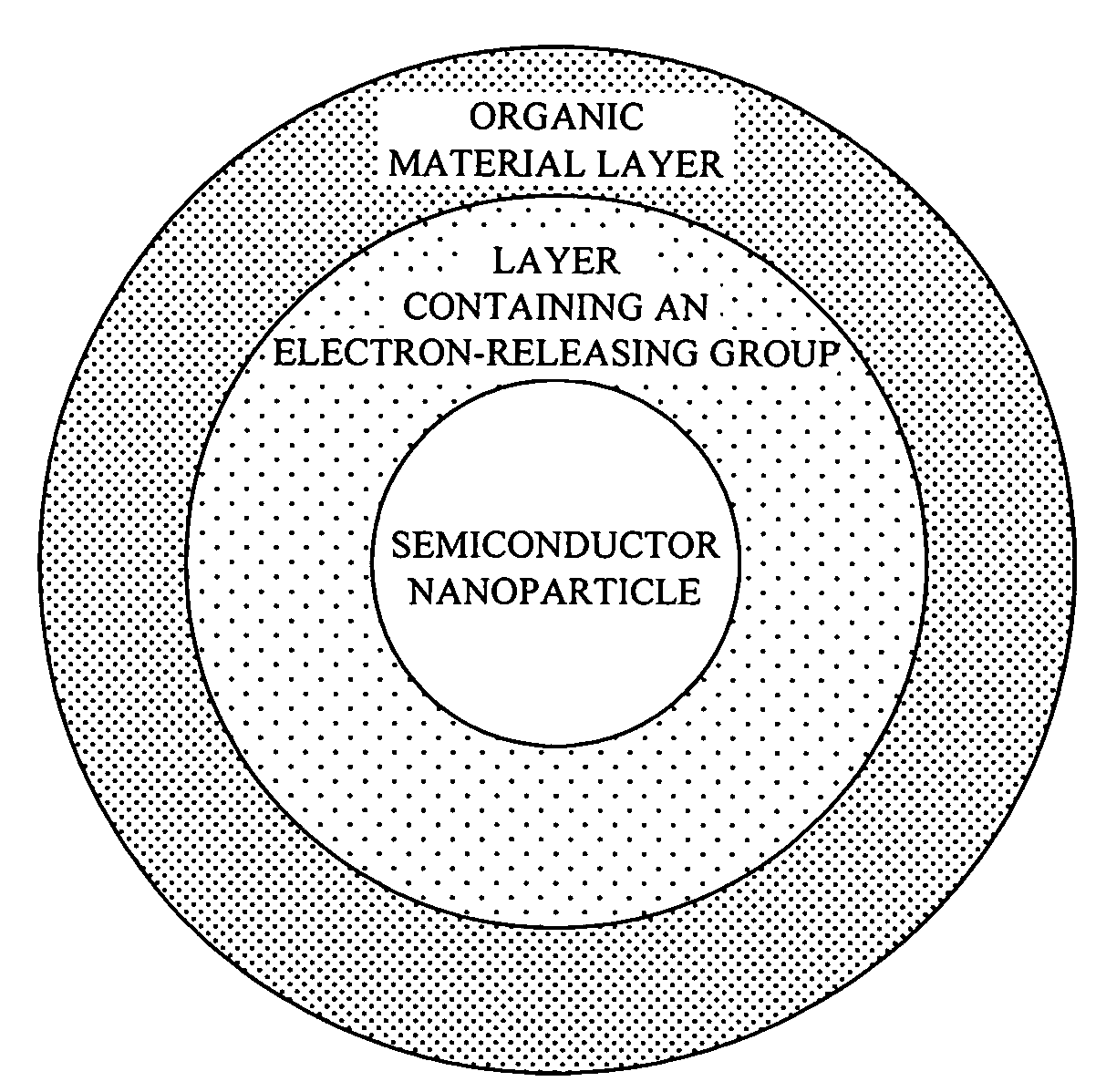
Organic material-coated semiconductor nanoparticle with excellent durability, and method of manufacturing the same
a technology of organic materials and semiconductors, applied in the field of nanoparticles, can solve the problems that the durability of the semiconductor nanoparticle provided with a surface treatment such as the oh coating or ammonia treatment is not sufficient, and achieves the effects of excellent durability, excellent durability, and excellent durability
- Summary
- Abstract
- Description
- Claims
- Application Information
AI Technical Summary
Benefits of technology
Problems solved by technology
Method used
Image

Examples
example 1-1
(Surface Treatment with Sodium Hydroxide)
[0084]In this example, the surface treatment employed sodium hydroxide.
[0085]The purified and thiol-modified nanoparticle aqueous solution obtained as described above was diluted to an absorbance of 0.5 using 0.1 M NaOH—HCl, ph 11 aq. The solution was allowed to stand for several days to several weeks to treat the surface, thereby obtaining a semiconductor nanoparticle solution with high-emission properties. The resultant solution was optically transparent yellow and had superior emission properties.
example 1-2
[0086]In this example, the surface treatment employed ammonia water.
[0087]The purified and thiol-modified nanoparticle aqueous solution obtained as described above was diluted to an absorbance of 0.5 using 0.1 M NH3 aq. The solution was allowed to stand for several days to several weeks to treat the surface, thereby obtaining a semiconductor nanoparticle solution with high-emission properties. The resultant solution was optically transparent yellow and had superior emission properties.
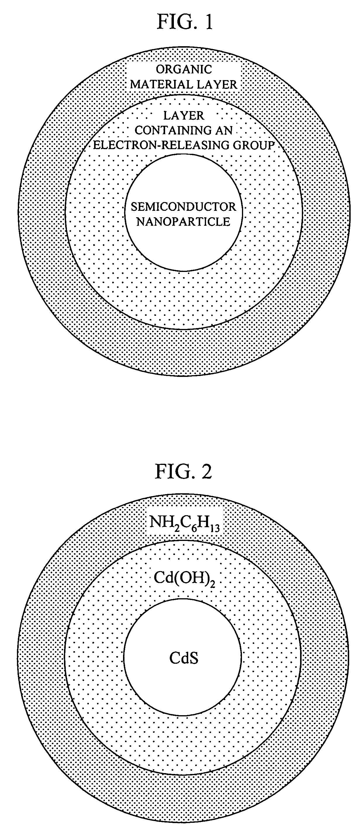
Method of Coating the Surface of Semiconductor Nanoparticles
example 2-1
NaOH Treatment / Hexylamine / Toluene
[0088]A mixture solution of toluene and hexylamine, the latter of an amount that was 10% that of the former, was added to an equal amount of the semiconductor nanoparticle aqueous solution prepared in Example 1-1. After violently stirring for some time, it was confirmed that an optically transparent yellow portion migrated from an aqueous phase to an organic phase through a stage in which a yellow powdery substance was observed at the water-toluene interface. Thereafter, centrifugation was carried out and the aqueous phase and the organic phase were separated. The recovered organic phase was then diluted by adding toluene to the same amount as the amount of the aforementioned aqueous solution prior to migration. The semiconductor nanoparticles that migrated to a toluene phase still maintained high-emission properties.
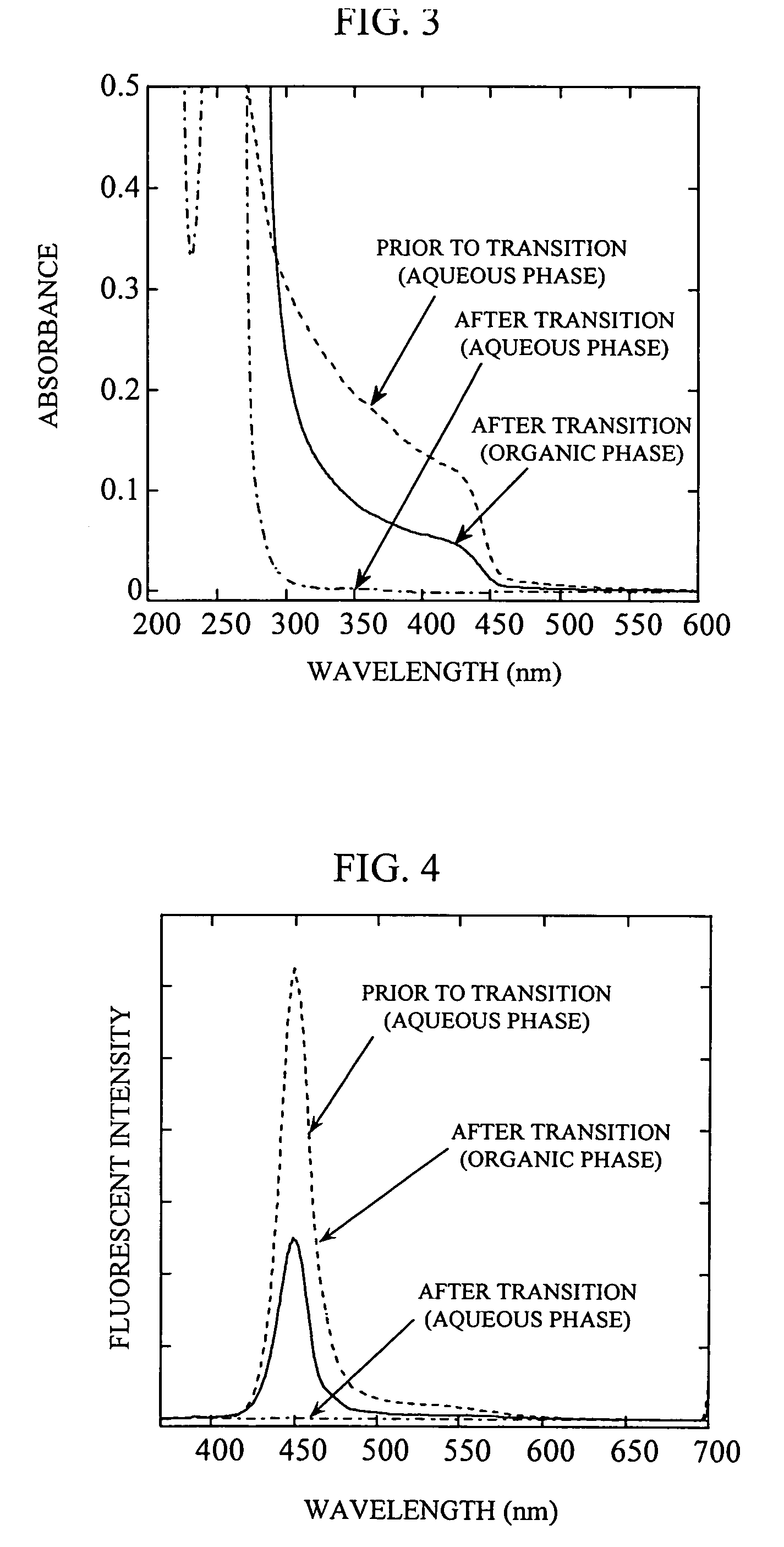
[0089]The structure of the resultant semiconductor nanoparticles is schematically shown in FIG. 2. FIG. 3 shows the absorption spectra ...
PUM
| Property | Measurement | Unit |
|---|---|---|
| FWHM | aaaaa | aaaaa |
| particle sizes | aaaaa | aaaaa |
| particle size distribution | aaaaa | aaaaa |
Abstract
Description
Claims
Application Information