Method of maintaining signal integrity across a capacitive coupled solder bump

a capacitive coupled and solder bump technology, applied in the direction of electronic circuit testing, measurement devices, instruments, etc., can solve the problems of no way to test or even use the dut, formation or collection of resistive and capacitive substances, such as oxides, on the surface of electrical contacts

Inactive Publication Date: 2008-01-15
ALTERA CORP
View PDF18 Cites 31 Cited by
  • Summary
  • Abstract
  • Description
  • Claims
  • Application Information

AI Technical Summary

Benefits of technology

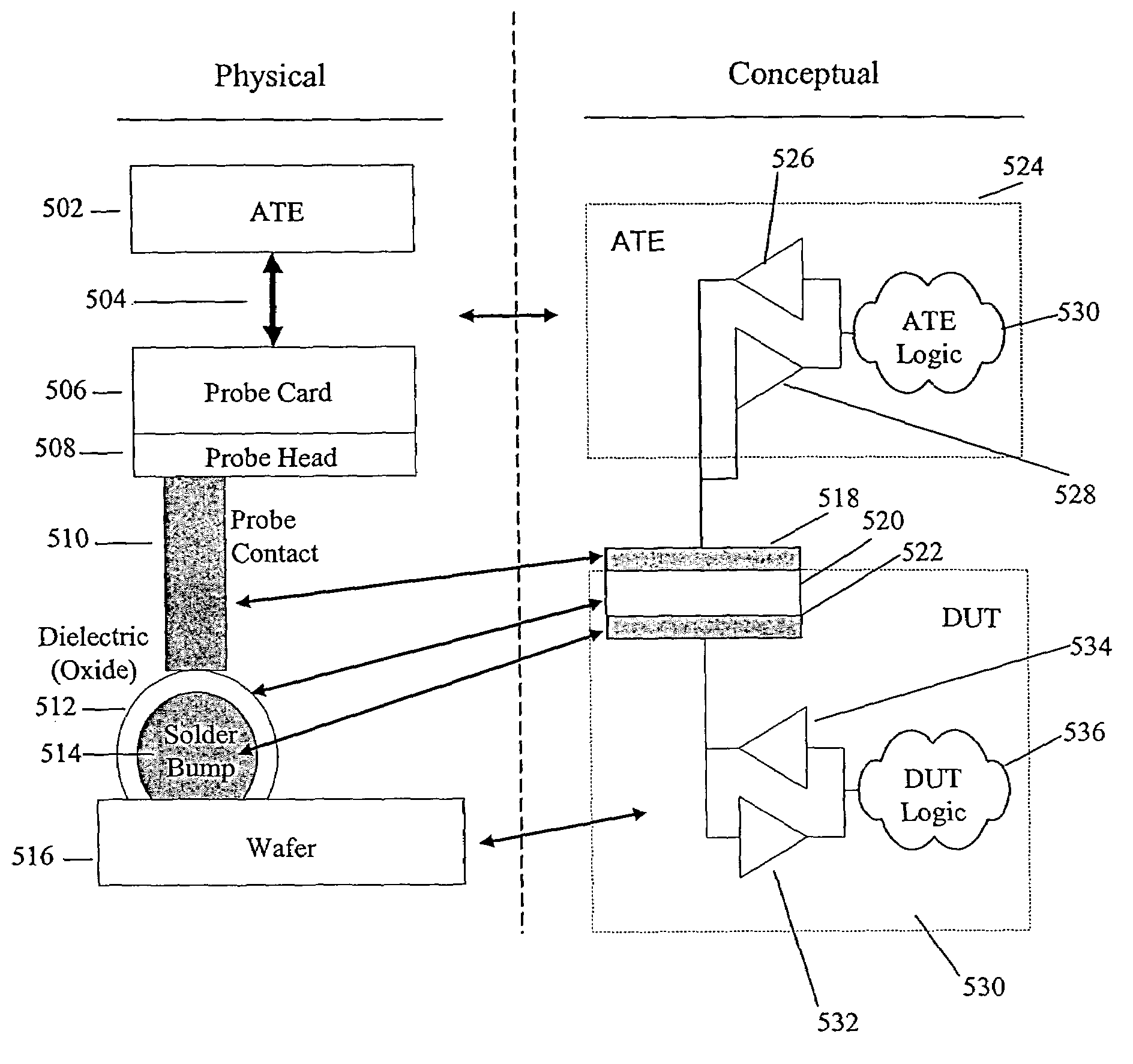
[0014]The present invention includes a process of testing an electronic device by moving the device in a first direction such that physical contact is made between one or more of the solder bumps on the device and one or more of the metal probe card contacts coupled to the test system. Typically, even after other cleaning techniques are applied, a subset of the solder bumps include a dielectric layer covering a portion of a surface of the solder bumps such that a capacitor is formed at the interface between the metal probe card contact, the dielectric layer and the solder bumps within the subset. Using the capacitive characteristics of the interface capacitor, the device is tested. This process may further include applying an initial voltage signal across the interface capacitor to test the device, capturing a voltage response from the device, and comparing the voltage response to an expected response. If the voltage response does not match the expected response, then one or more voltage parameters in a testing system coupled to the probe card contacts may be adjusted. The one or more voltage parameters are adjusted to pre-determined limits until the voltage response matches the expected response, or else the device fails

Problems solved by technology

With or without BST architecture, an error is found when the actual response signals from the DUT do not match the expected signals.
In other words, if signals cannot effectively get from the tester into the DUT circuit and vice versa, there is no way to test or even use the DUT.
A significant problem in this regard is the formation or collection of resistive and capacitive substances, such as oxides, on the surface of the electrical contacts of the DUT.
An added capacitance and resistance may slow the transmission of signals to and from the device such that the device will not function at a 200 MHz speed.
An oxide may cause false negatives in the testing of DUTs, and it may require that the tests be repeated.
Testing devices is a time consuming and expensive activity, and requiring multiple tests only increases the time and expense.
Additionally, the probe card contacts have a limited life, and multiple tests on each wafer will degrade the probe contacts that much faster.
These add to the testin

Method used


Image

  • Method of maintaining signal integrity across a capacitive coupled solder bump
  • Method of maintaining signal integrity across a capacitive coupled solder bump
  • Method of maintaining signal integrity across a capacitive coupled solder bump

Examples


example

[0086]The following tables show examples of various test parameters and pass / fail results for sample DUTs. Tables 1 and 2 are examples of the application of relationships (5) and (6), respectively. Table 1 illustrates examples wherein the ATE is the driver and a DUT is the load, and Table 2 illustrates examples of the reverse path. The epsilon used is an approximate one assuming lead-oxide, and includes both the permittivity constant (∈0) and the permittivity multiplier (∈) for lead oxide. CI is calculated using relationship (7), with oxide thickness as the distance (d) between the two conducting plates. Contact areas are typical for solder bumps contacted by flat-tipped probe contacts.

[0087]

TABLE 1OxideVOHATE >VOHATEVIHDUTCDUTEpsilonContactthicknessCIVIHDUT *(V)(V)(pF)(F / m)area (m2)(m)(pF)(1 + CDUT / CI)13.31.7102.2e-101.26e-93e-08 9.3Fail23.71.7102.2e-101.26e-93e-08 9.3Pass33.31.4102.2e-102.83e-93e-0820.9Pass

[0088]

TABLE 2OxideVOHDUT >VOHDUTVIHATECATEEpsilonContactthicknessCIVIHATE *...


PUM


Abstract

The present invention is a novel method and computer program product which utilizes an interface capacitor formed by the metal of the probe tip, a dielectric layer, such as an oxide, formed by a contaminant on a solder bump and the metal of the solder bump. The interface capacitor forms a capacitive divider with the inherent capacitances of the automatic test equipment and the device under test (DUT). The voltage characteristics of the capacitive divider are used to drive voltage signals across the interface capacitor to test the DUT. In either direction (i.e. from the automatic test equipment to the DUT or vice versa), by altering the voltage output high amplitude of the driver and/or the voltage input high amplitude of the load, the DUT is validly tested through the interface capacitor. Thus, even if all I/O bumps have an oxide layer, the device may still be validly tested.

Description

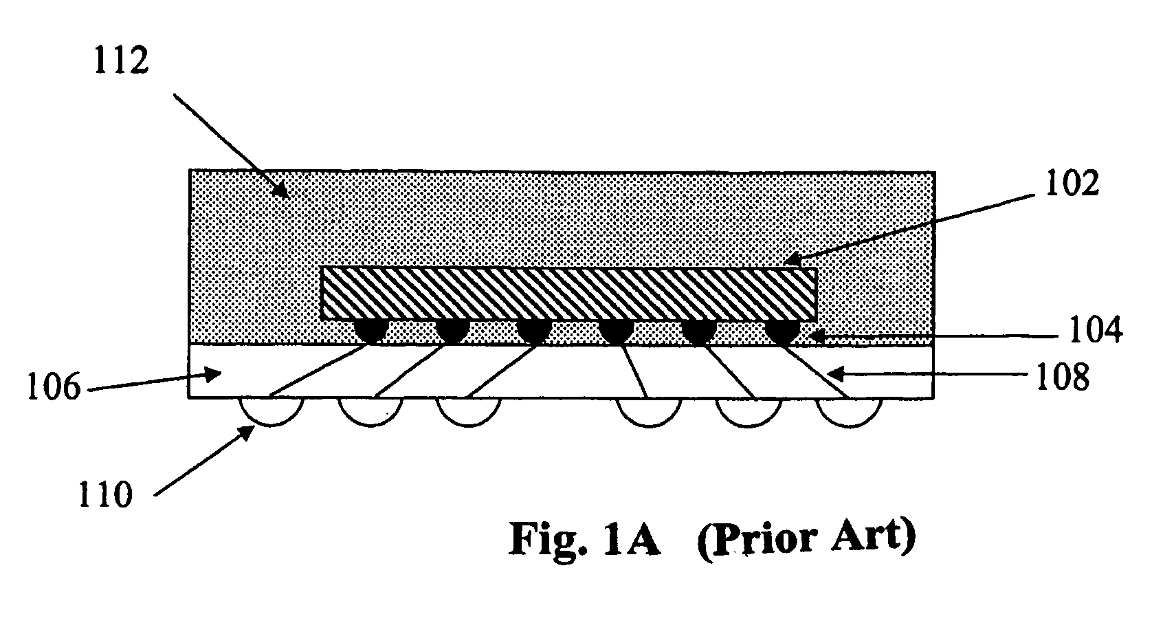
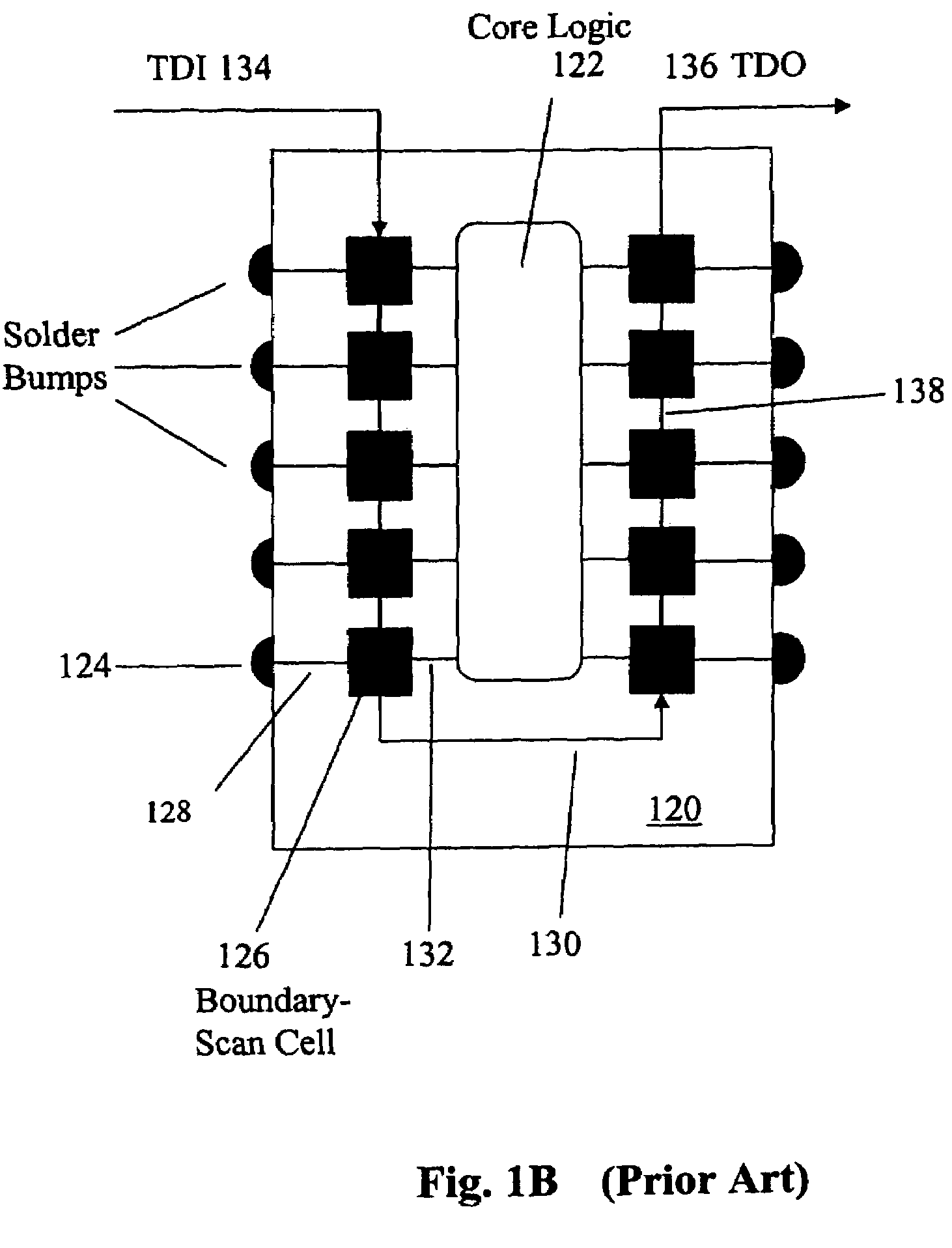
[0001]The present invention relates generally to maintaining electrical signal integrity during the testing of integrated circuits, and particularly to the manufacturing testing of flip chip integrated circuits with solder bumps.BACKGROUND OF THE INVENTION[0002]This invention is especially useful in testing flip-chip devices. As shown in the illustration of a single flip-chip device 102 in FIG. 1A, such flip-chip devices typically have solder bumps 104 on a face of the flip-chip that are the electrical connections to the flip-chip 102. The flip-chip 102 is encapsulated in a larger package 112; and solder bumps 104 are connected via connectors schematically represented by lines 108 through a packaging substrate 106 to larger package solder bumps 110 (e.g. in a Ball Grid Array (BGA) configuration). The package solder bumps 110 are used to connect the entire package to a printed circuit board (PCB) or other electronic device. The solder bumps 104 of the flip-chip 102 are critical to th...

Claims


Application Information

Patent Timeline
IPC IPC(8): G01R31/26
CPCG01R1/06794
Inventor HARMS, MICHAELCHANG, ERIC C.TRACY, PAULDICOSOLA, JOHNBRAHMACHARI, MANDRITA
Owner ALTERA CORP
Why Eureka
Try Eureka