Hybrid linear wire model approach to tuning transistor widths of circuits with RC interconnect

a technology of rc interconnect and wire model, which is applied in the direction of cad circuit design, program control, instruments, etc., can solve the problems of delay, power, area, delay or power of design, inability to adjust etc., and achieve the effect of optimizing the width of the transistor

Active Publication Date: 2008-01-29
GLOBALFOUNDRIES U S INC
View PDF24 Cites 17 Cited by
  • Summary
  • Abstract
  • Description
  • Claims
  • Application Information

AI Technical Summary

Benefits of technology

[0010]Accordingly, it is an object of the invention to optimize the widths of transistors in an integrated circuit while accounting for the effect on the circuit timing of the parasitic RC networks interconnecting the transistors.
[0011]It is another object to perform the above mentioned optimization in a speedy manner without significant loss of accuracy.
[0012]The present invention fully utilizes the strengths and hides the weaknesses of both types of embedded circuit simulators: the Timing oriented simulator that efficiently performs the transient analysis of a circuit including resistors used in the pre-tuning phase, and the Gradient oriented simulator that efficiently computes, in the iterative tuning phase, the sensitivities (or gradients) in a circuit devoid of resistors. The invention uses the results of the pre-tuning phase to correct the effect of the Rs in the interconnect wiring ignored during the tuning phase.
[0013]Since there is no suitable embedded simulator within the tuner to run directly on an extracted RC netlist, a ‘hybrid’ approach is described wherein all the parasitic interconnects are accounted for during the circuit optimization phase by exploiting the strengths of both types of available embedded simulators, namely, a Timing oriented simulator which is fast and accurate for timing circuits that include Rs (even with a wide dynamic range in values) as long as it is not required to compute sensitivities, and a Gradient oriented simulator which is fast and accurate for both timing and sensitivity calculations as long as no Rs are present in the circuit being analyzed.

Problems solved by technology

Other constraints may enforce design requirements on the final optimization result, such as limits on the area, delay, or power of the design.
In current technologies, circuit designers have found that ignoring the resistance (R) of the interconnect wiring when tuning the widths of the transistors causes unacceptable loss of accuracy.
The delay of the interconnect (referred to hereinafter as RC delay) is becoming more significant as devices become smaller, as the technology advances, and as the design cycle time is pushed to even faster limits.
Unfortunately, the presence of Rs in the interconnections is a major obstacle when using currently available embedded simulators either during timing or during the sensitivity computation.
Unfortunately, while this simulator is fast and accurate when used for timing circuit with Rs, it is too slow and inaccurate to use for computation of sensitivities in such circuits.
Unfortunately, the Gradient oriented simulator is too slow even for timing circuits when Rs are present.
A problem remains unresolved in that no embedded simulators exist that are sufficiently fast and accurate for performing both timing and sensitivity calculations on circuits in the presence of Rs in the interconnect wiring.
The large number of Rs increases the size of the circuit sent to the embedded simulator while the wide dynamic range in the resistor values causes a phenomenon know as stiffness in the differential equations solved by the simulator, leading to a significant slow-down in the simulator.

Method used


Image

  • Hybrid linear wire model approach to tuning transistor widths of circuits with RC interconnect
  • Hybrid linear wire model approach to tuning transistor widths of circuits with RC interconnect
  • Hybrid linear wire model approach to tuning transistor widths of circuits with RC interconnect

Examples


Embodiment Construction

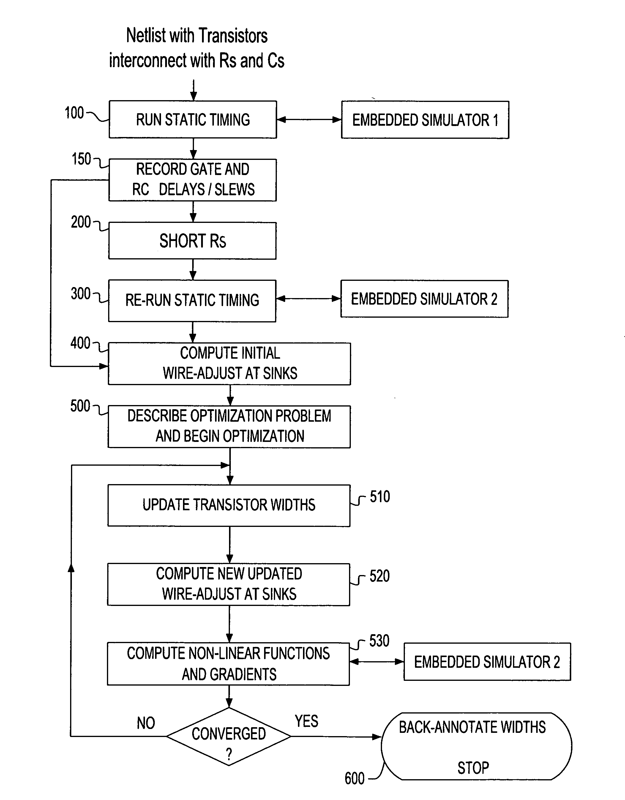
[0020]Referring now to FIG. 4, there is shown a flow chart outlining the various steps of the ‘hybrid’ simulator approach of the present invention. The method detailed hereinafter is applied to a circuit design described by a netlist that includes interconnect wiring that includes both Rs and Cs.

[0021]In step 100, a static transistor-level timer for timing the netlist computes the timing information by running the Timing oriented simulator (also referred to, for simplicity, as Simulator 1).

[0022]In step 150, in an operation referred to as the pre-tuning phase, the gate delay and slew and RC delay and slew information of each stage is recorded. The gate delay is the delay from the stage input to the output node of the gate. An RC delay is the delay from the gate output (which is also the source node of the interconnect network) to a net sink, and there will generally be a different RC delay for each net sink. The widths of all the transistors become the initial values of the netlist....


PUM


Abstract

A hybrid linear wire model for tuning the transistor widths of circuits linked by RC interconnects is described. The method uses two embedded simulators during the tuning process on netlists that contain resistors (Rs). A Timing oriented simulator is used only for timing purposes on the original netlist that includes all the Rs. A Gradient oriented simulator is then run only on the modified netlist with all Rs shorted and within the iterative loop of the tuner to compute gradients. The present hybrid method achieves a significant improvement in computational speed. The Timing oriented simulator is fast and accurate for only timing netlists with Rs, but cannot compute gradients efficiently. The Gradient oriented simulator computes gradients efficiently but cannot do so in the presence of Rs. To prevent “de-tuning” that typically occurs when all Rs are shorted, ‘wire-adjusts’ are provided that make the initial timing results using the Gradient oriented simulator on the shorted netlist match the timing results using Timing oriented simulator on the original netlist. This permits the optimizer sense initially the correct set of critical timing paths, and more significantly, it permits the wire-adjusts keep track of the changing transistor widths to guide the optimizer during the iterations until convergence is achieved.

Description

BACKGROUND OF THE INVENTION[0001]This invention is related to the field of Electronic Design Automation, and more particularly, to a method for optimizing the widths of transistors in an integrated circuit (IC) while accounting for the effect of the interconnect resistors and capacitors (RC) on the timing of the circuit.[0002]Integrated circuits are typically modeled to perform electrical analysis using for this purpose a netlist of transistors (referred to hereinafter as switching devices) interconnected by linear circuit elements, such as resistors (Rs) and capacitors (Cs). The widths of the transistors affect the performance (speed, area, power, etc.) of the circuit. The so-called ‘Transistor Widths Tuning’ problem involves assigning optimal values to the transistor widths to achieve the best possible performance, such as minimal area, minimal cycle time, and the like.[0003]A variety of approaches has been used in industry to solve the tuning problem. One approach utilizes a gene...

Claims


Application Information

Patent Timeline
Patent Type & Authority Patents(United States)
IPC IPC(8): G06F17/50
CPCG06F17/5031G06F17/5045G06F17/5068G06F30/3312G06F30/39G06F30/30G06F2119/12
Inventor RAO, VASANTWASHBURN, CINDYZHOU, JUNSOREFF, JEFFREY P.WILLIAMS, PATRICK M.HATHAWAY, DAVID J.
Owner GLOBALFOUNDRIES U S INC
Why Eureka
Try Eureka