Micro sensor for electrochemically monitoring residue in micro channels

Inactive Publication Date: 2008-02-19
ENVIRONMENTAL METROLOGY CORP
View PDF5 Cites 44 Cited by
  • Summary
  • Abstract
  • Description
  • Claims
  • Application Information

AI Technical Summary

Benefits of technology

[0013]The present invention provides a micro sensor for monitoring the cleaning and drying processes for high aspect ratio micro channels in dielectric films oriented parallel to the fluid-solid interface during the manufacture of ICs, MEMS and other micro devices. The micro sensor can be used to monitor “vertical” micro features common in microelectronics fabrication or “horizontal” micro features found in MEMS

Problems solved by technology

A major challenge in manufacturing of the micro and nano devices is the cleaning and drying of very small void features (“micro features”), particularly those with large aspect ratios.
Cleaning and drying occur repeatedly during the processing chain and are responsible for a significant part of the total processing time and for the consumption of much of the water, chemicals and energy.
Most of these features have high aspect ratios with submicron openings and are therefore very difficult to clean and dry.
Improper cleaning and drying would have a significant effect on manufacturing yield and device performance and reliability in both semiconductor and MEMS fabrication.
Over-cleaning, over-rinsing or over-drying results in excessive use of chemicals, water and energy and also increases cycle time and potentially causes yield loss.
The key reason for this inefficient and costly approach is that no sensors or techniques are available to measure the cleanliness and monitor the removal of impurities from micro features—to measure cleanliness where it actually counts.
The present monitoring techniques and devices do not provide realistic and accurate information on the cleanliness and condition of micro

Method used


Image

  • Micro sensor for electrochemically monitoring residue in micro channels
  • Micro sensor for electrochemically monitoring residue in micro channels
  • Micro sensor for electrochemically monitoring residue in micro channels

Examples


Example

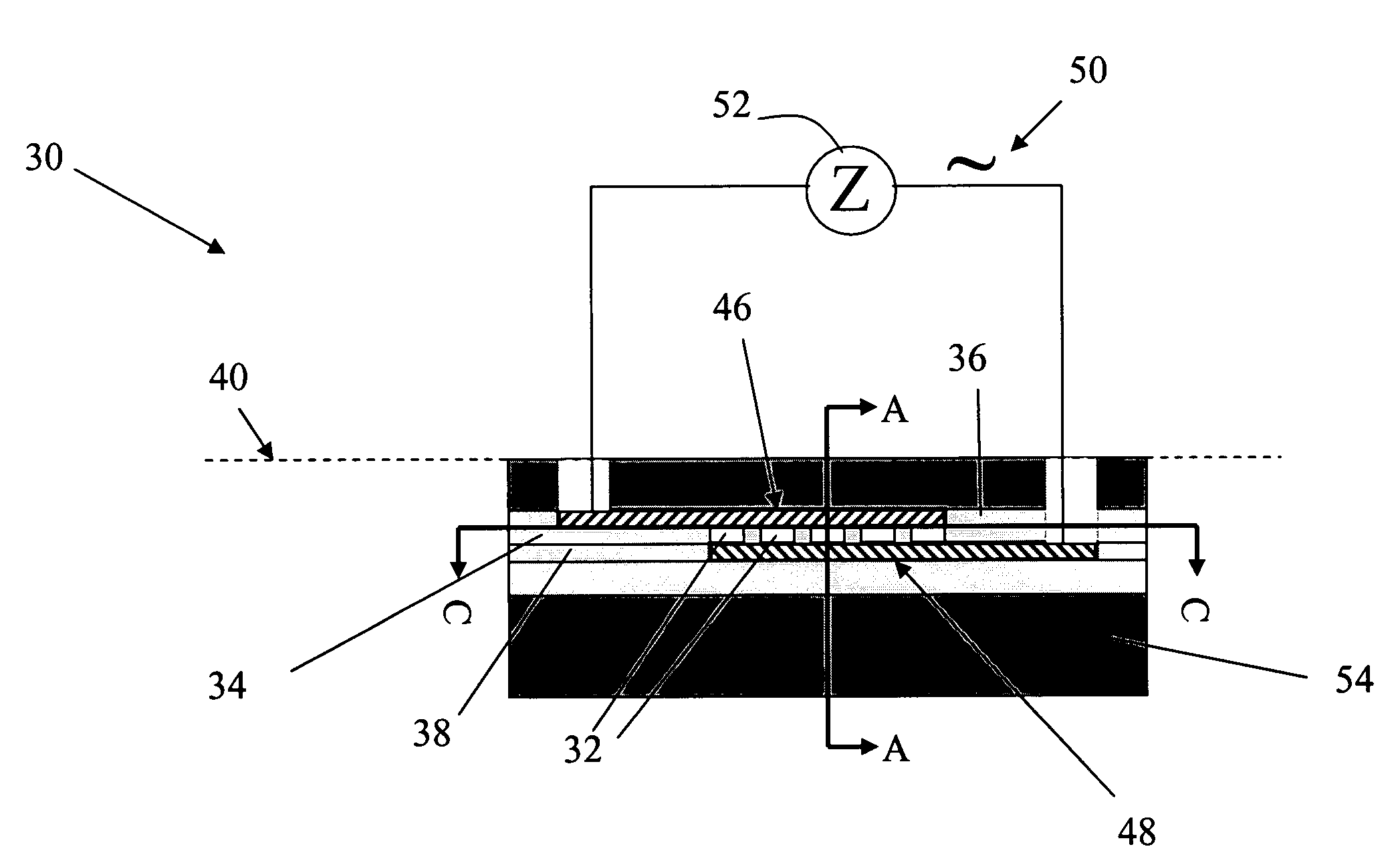
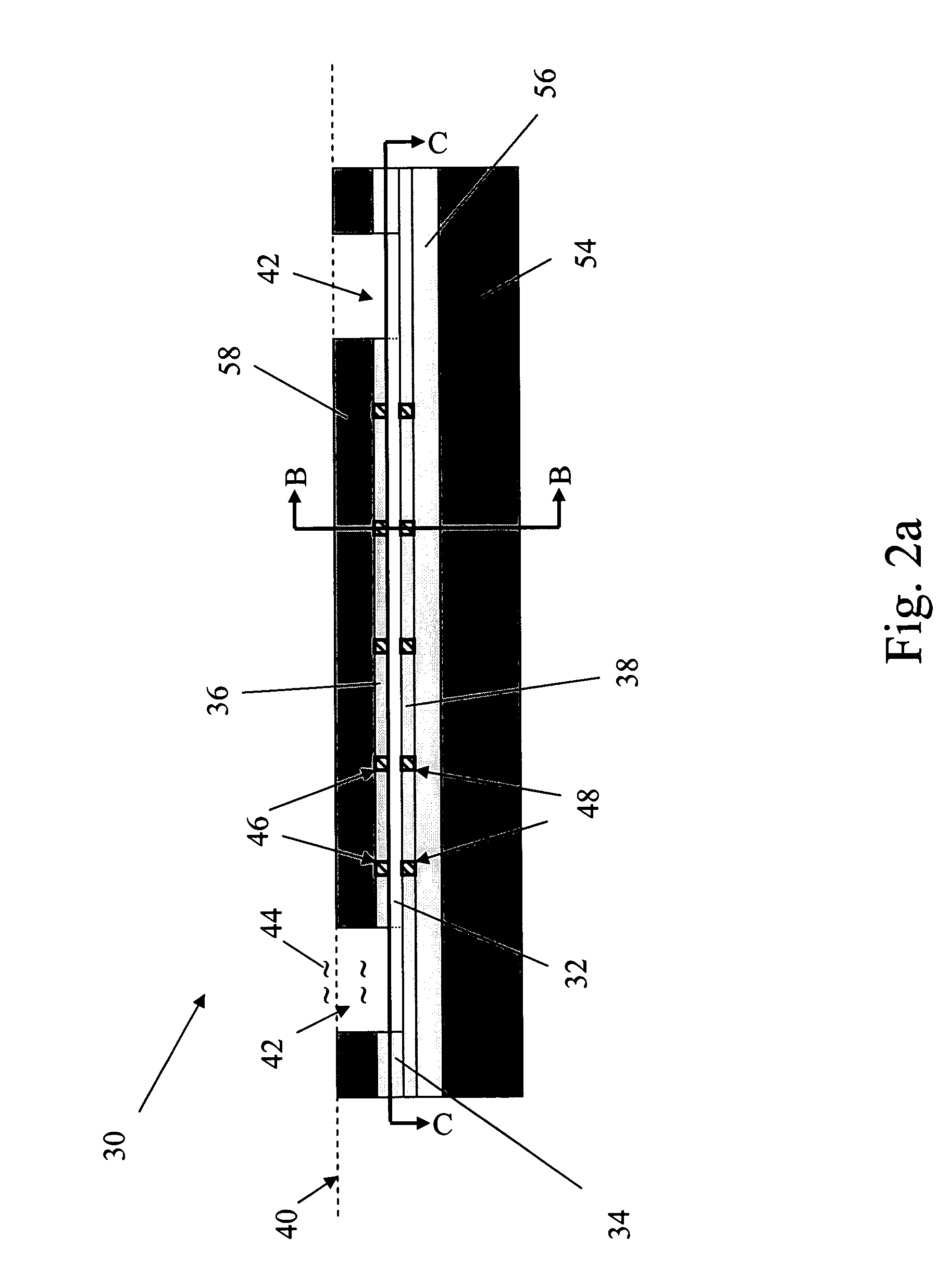
[0029]The present invention provides a micro sensor for monitoring the cleaning and drying processes for high aspect ratio micro features in dielectric films during the manufacture of ICs, MEMS and other micro devices. The term “micro feature” is used to refer to both “horizontal” and “vertical” (with respect to the substrate) void micro features such as trenches, vias, holes, pores, etc. These void micro features have aspect ratios of greater than 1:1, typically at least 3:1 and potentially much larger. The micro feature may be filled with a porous dielectric material as well.

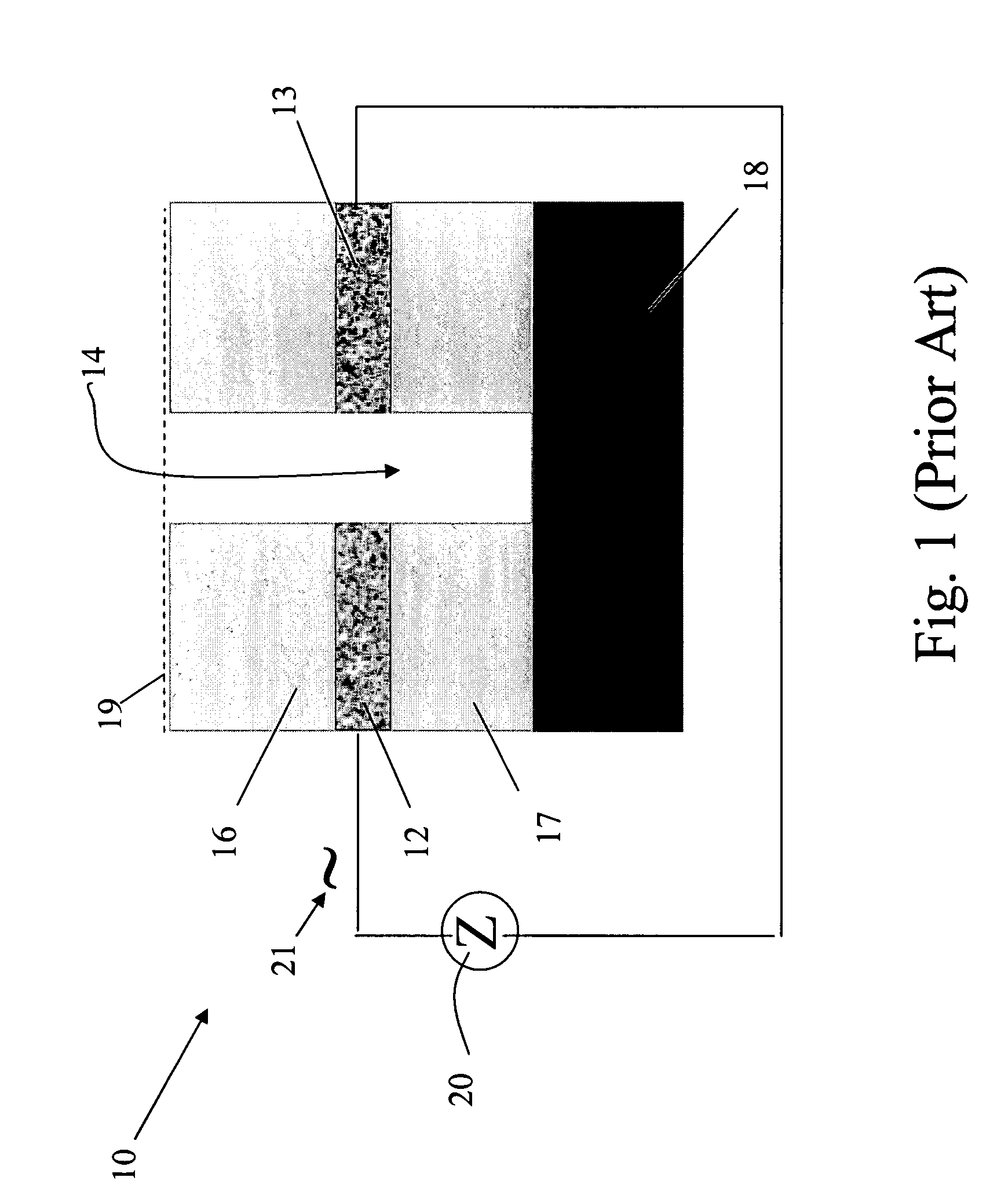
[0030]The term “micro channel” is used to refer to the void micro structure formed parallel to the fluid-solid interface that is used to emulate and thus monitor in-situ micro features in semiconductor, MEMS and microfluidic devices. By forming the micro channels substantially parallel to the interface, the channels can be made with much higher and well controlled aspect ratios. The aspect ratio of a micro cha...


PUM

PropertyMeasurementUnit
Dielectric polarization enthalpyaaaaaaaaaa
Aspect ratioaaaaaaaaaa
Electric impedanceaaaaaaaaaa

Abstract

The present invention provides a micro sensor for monitoring the cleaning and drying processes for very high aspect ratio micro channels in dielectric films oriented parallel to the fluid-solid interface during the manufacture of ICs, MEMS and other micro-devices. The micro sensor can be used to monitor “vertical” micro features common in microelectronics fabrication or “horizontal” micro features found in MEMS or microfluidic fabrication. By forming the micro channels parallel to the interface, the channels can be made with much higher and well controlled aspect ratios. In addition, multiple sensors can sense the impedance at various points along the micro features. The addition of a guard reduces the effects of any parasitic capacitance, which extends the measurement bandwidth of the sensor.

Description

CROSS-REFERENCE TO RELATED APPLICATIONS[0001]This application claims benefit of priority under 35 U.S.C. 119(e) to U.S. Provisional Application No. 60 / 624,131 entitled “Method For Impedance Monitoring Of Fluids And Gases In High Aspect Ratio Structures And Method For Manufacturing Such A Monitor” filed on Nov. 2, 2004, the entire contents of which are incorporated by reference.BACKGROUND OF THE INVENTION[0002]1. Field of the Invention[0003]This invention relates to monitoring the cleaning and drying processes during the manufacture of ICs, MEMS and other micro devices and more specifically to a micro sensor for high aspect ratio micro channels in dielectric films oriented parallel to the fluid-solid interface to emulate either “vertical” or “horizontal” micro features.[0004]2. Description of the Related Art[0005]A major challenge in manufacturing of the micro and nano devices is the cleaning and drying of very small void features (“micro features”), particularly those with large asp...

Claims


Application Information

Patent Timeline
IPC IPC(8): G01N27/00G01N27/26G01R27/28
CPCB01L3/5027G01N27/07B01L2300/0887B01L2300/0645B01L2300/0816B01L3/502707
Inventor VERMEIRE, BERT M.SHADMAN, FARHANG F.
Owner ENVIRONMENTAL METROLOGY CORP
Why Eureka
Try Eureka