Two-dimensional photonic crystal having air-bridge structure and method for manufacturing such a crystal

a technology of photonic crystal and air bridge, which is applied in the direction of manufacturing tools, instruments, optical elements, etc., can solve the problems of low product yield, low product yield, and the loss of light, and achieve the effect of minimizing the loss of ligh

Inactive Publication Date: 2008-02-19
KYOTO UNIV
View PDF20 Cites 25 Cited by
  • Summary
  • Abstract
  • Description
  • Claims
  • Application Information

AI Technical Summary

Benefits of technology

[0021]The second problem to be addressed by the present invention is to provide a method for manufacturing a two-dimensional photonic crystal having a wire waveguide in which the slab of the two-dimensional photonic crystal is in contact with air on both the upper and lower sides whereas the wire waveguide connected to the two-dimensional photonic crystal is supported by a clad member. Particularly, the present invention intends to provide a manufacturing method free from positional discrepancy between the in-crystal waveguide and the wire waveguide of the two-dimensional photonic crystal.Means for Solving the Problems
[0077]The third mode of the manufacturing method according to the present invention yields the following effects: According to the present invention, the wire waveguide is formed outside the air-bridge space, which has already been formed. Therefore, the lower side of the wire waveguide securely comes in contact with the clad layer. The guided mode of the wire waveguide thus manufactured is the single mode, which will never cause any problem associated with the multimode. In addition, the two-dimensional photonic crystal is created over the air-bridge space, which has already been formed. Therefore, the lower side of the two-dimensional photonic crystal securely comes in contact with the air-bridge space. The difference in the refractive index between the two-dimensional photonic crystal and the air existing on its upper and lower sides makes it possible to confine the light in the direction perpendicular to the slab and thereby minimize the loss of light. Furthermore, since the in-crystal waveguide and the wire waveguide are formed in the same process, there is no need to adjust the positions of the in-crystal waveguide and the wire waveguide. The wire waveguide will be correctly formed on the extension of the in-crystal waveguide.

Problems solved by technology

Particularly, two-dimensional photonic crystals created by forming a number of holes in the slab are very fragile in the thickness direction.
Lack of the strength in the thickness direction will cause some problems, such as a low level of product yield.
Therefore, the substrate-attached photonic crystal is less advantageous than the substrate-less photonic crystal with respect to the wavelength resolution of the resonator.
Such a multimode propagation may cause some problems in optical communications.
However, if the etching is performed to create an air-bridge space under the two-dimensional photonic crystal section of the two-dimensional photonic crystal having the wire waveguide manufactured as described above, the problem arises that the etchant infiltrates into the clad layer through the vicinity of the wire waveguide and etches the clad layer under the wire waveguide as well as under the two-dimensional photonic crystal.
Furthermore, due to the lack of strength, the wire waveguide may be broken.
Putting a protective mask around the wire waveguide cannot perfectly prevent the infiltration of the etchant through the gap between the wire waveguide and the mask; a portion of the clad layer under the wire waveguide will be etched.
In addition, a discrepancy may occur between the wire waveguide and the extension line of the in-crystal waveguide, which will deteriorate the light-guiding efficiency between the in-crystal waveguide and the wire waveguide.

Method used


Image

  • Two-dimensional photonic crystal having air-bridge structure and method for manufacturing such a crystal
  • Two-dimensional photonic crystal having air-bridge structure and method for manufacturing such a crystal
  • Two-dimensional photonic crystal having air-bridge structure and method for manufacturing such a crystal

Examples


embodiment 1

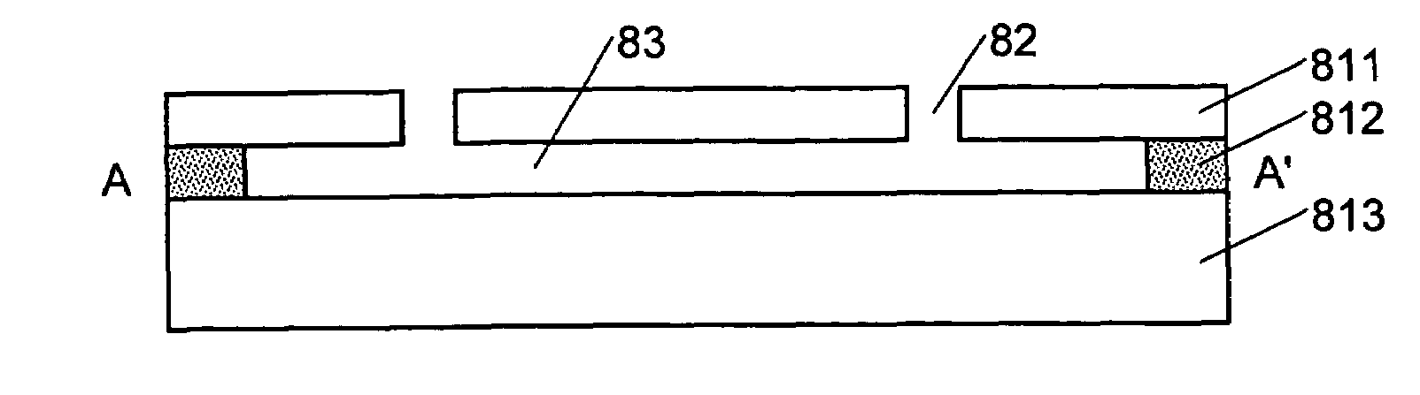
[0119]FIG. 6 shows an example of the structure of the two-dimensional photonic crystal having an air-bridge space facing a point-like defect, where (a) is a perspective view, (b) is a plan view, and (c) shows the left side cross section at line A-A′ in (b) and the right side cross section at line B-B′. This device consists of a slab layer 31 made of silicon (Si), a clad layer 32 made of SiO2, and a silicon layer 33 made of Si. The clad layer 32 combined with the silicon layer 33 supports the slab layer 32.

[0120]In the slab layer 31, holes 35 are cyclically arranged in a triangular lattice pattern. This structure has a photonic bandgap and prevents rays of light having wavelengths corresponding to the energy levels within the photonic bandgap from propagating through the body layer. In the present case, the cycle a of the triangular lattice is 0.41 μm. A point-like defect 36 is formed by eliminating three holes 35 along a straight line, or by omitting the three holes. An air-bridge s...

embodiment 2

[0125]An embodiment of the method for manufacturing the two-dimensional photonic crystal of the first mode is described with reference to FIG. 11.

[0126]The present method uses an SOI substrate 41 composed of three layers: a slab layer 31 made of Si, a clad layer 32 made of SiO2 and a silicon layer 33 made of Si. Commercial SOI substrates can be used as the SOI substrate 41. First, two etchant introduction holes 42 are bored in the slab layer 31 (a). The etchant introduction holes 42 are formed, for example, by the steps of applying an electron beam resist on the slab layer 31, writing images of the etchant introduction holes 42 using an electron beam, and performing a dry etching process using an etching gas (e.g. SF6). Next, the SOI substrate 41 is dipped into an aqueous solution of hydrogen fluoride 43 (b). The aqueous solution of hydrogen fluoride entering through the etchant introduction holes 42 etches only the clad layer 32 without affecting the slab layer 31 and the silicon l...

embodiment 3

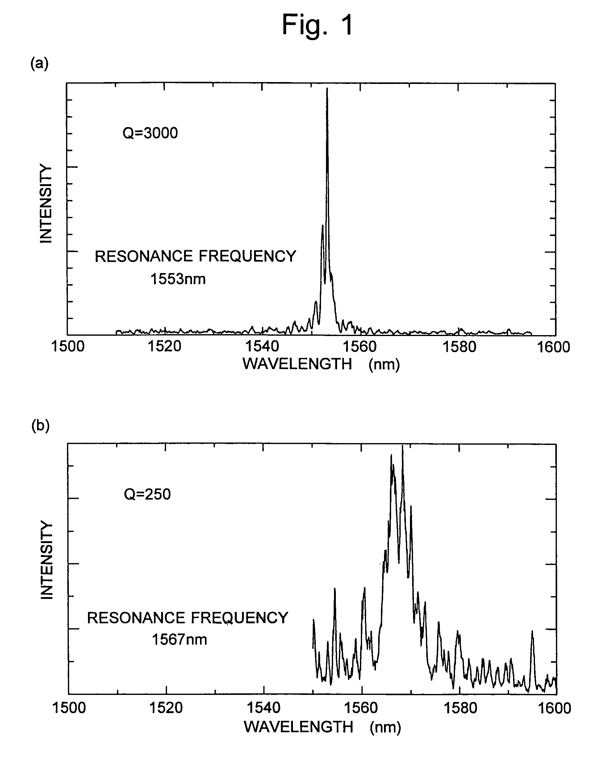
[0131]The waveguide transmission band of a waveguide located over an air-bridge space was analyzed using a two-dimensional photonic crystal having an air-bridge structure. The result is as follows:

[0132]If, as shown in FIG. 14(a), the width of the waveguide is uniform (1.11 times the cycle a of the holes 51) within both the area 501 over the SiO2 substrate layer and the area 502 over the air-bridge space 52, the common band (i.e. the wavelength band within which light is allowed to pass through both areas 501 and 502) will be as denoted by numeral 531 in FIG. 14(b), where the coordinate indicates the normalized frequency (the frequency of light multiplied by the cycle of the holes 51 and divided by the speed of light) and the abscissa indicates the wave number of light. The shaded area shows the frequency band inappropriate for the waveguide transmission band because it allows the TM wave to be coupled with the TE wave within the waveguide and leak in in-plane directions.

[0133]In co...


PUM

PropertyMeasurementUnit
thicknessaaaaaaaaaa
thicknessaaaaaaaaaa
thicknessaaaaaaaaaa

Abstract

The present invention intends to provide a two-dimensional photonic crystal having a high level of mechanical strength and functioning as a high-efficiency resonator. The two-dimensional photonic crystal according to the present invention includes a slab layer 31 under which a clad layer 32 is located. In the slab layer 31, areas 35 having a refractive index different from that of the slab layer 31 are cyclically arranged to create a two-dimensional photonic crystal. A portion of the cyclic arrangement of the areas 35 are omitted to form a point-like defect 36. This defect 36 functions as a resonator at which a specific wavelength of light resonates. An air-bridge cavity 37 facing the point-like defect 36 is formed over a predetermined range of the clad layer 32. In this construction, the clad layer 32 supports the slab layer 31 except for the range over which the air-bridge space 37 is formed. Therefore, the two-dimensional photonic crystal has a high level of mechanical strength. The presence of the air-bridge space 37 under the point-like defect 36 makes it easy to confine light at the point-like defect 36 by the difference in the refractive index between the slab layer 31 and the air. Thus, the point-like defect 36 functions as a high-performance resonator.

Description

TECHNICAL FIELD[0001]The present invention relates to a two-dimensional photonic crystal applicable for an optical multiplexer / demultiplexer, or similar devices, used in wavelength division multiplexing communication or other technologies. Particularly, it relates to a two-dimensional photonic crystal having a structure in which a slab of the two-dimensional photonic crystal is located on a clad layer having a space partially formed inside, and a method for manufacturing such a device. In the present patent application, such a structure is called the “air-bridge structure” and the space is called the “air-bridge space.”BACKGROUND ART(1) Photonic Crystals[0002]Recently, photonic crystals, which are optical functional materials having a cyclic distribution of refractive index, have been gaining attention. A photonic crystal is characterized in that its cyclic distribution of refractive index forms a band structure with respect to the energy of light or electromagnetic waves, thereby c...

Claims


Application Information

Patent Timeline
Patent Type & Authority Patents(United States)
IPC IPC(8): G02B6/10C03B37/022C03B37/023C03B37/027G02B6/12G02B6/122G02B6/13
CPCB82Y20/00G02B6/12004G02B6/12007G02B6/1225G02B6/13
Inventor HATSUDA, RANKONODA, SUSUMUASANO, TAKASHITANAKA, YOSHINORIMIYAI, EIJI
Owner KYOTO UNIV
Why Eureka
Try Eureka