Semiconductor device, manufacturing method thereof, and electronic device

a semiconductor and manufacturing method technology, applied in semiconductor devices, solid-state devices, transistors, etc., can solve the problems of inability to achieve a level which can be put to practical use, large can the grain size of a crystalline semiconductor film crystallized by laser light, and large grain size of a crystalline semiconductor film. , to achieve the effect of damping and reducing the effective energy strength of the secondary laser ligh

Inactive Publication Date: 2008-03-04
SEMICON ENERGY LAB CO LTD
View PDF100 Cites 9 Cited by
  • Summary
  • Abstract
  • Description
  • Claims
  • Application Information

AI Technical Summary

Benefits of technology

[0024]3) a method of attenuating the effective energy strength of the secondary laser light by the substrate material on which the amorphous semiconductor film is formed, and making the effective energy strength of the secondary laser light relatively smaller than the effective energy strength of the primary laser light;
[0025]4) a method of sandwiching an insulating film between the substrate and the amorphous semiconductor film, damping the effective energy strength of the secondary laser light by the insulating film, and making it relatively smaller than the effective energy strength of the primary laser light;
[0026]5) a method of covering the top surface of the amorphous semiconductor film by an insulating film, making the reflectivity of the primary laser light on the top surface of the amorphous semiconductor film smaller, and making the effective energy strength of the primary laser light relatively larger than the effective energy strength of the secondary laser light;
[0027]6) a method of covering the amorphous semiconductor film by an insulating film, attenuating the effective energy strength of the primary laser light, and making it relatively smaller than the effective energy strength of the secondary laser light; and

Problems solved by technology

The problem drawing the most attention at present is how large can the grain size of a crystalline semiconductor film crystallized by laser light be made.
However, it is difficult to obtain a crystalline semiconductor film with a sufficiently large grain size by present techniques, and although there are reports of such films being obtained experimentally, at present this has not reached a level which can be put to practical use.

Method used


Image

  • Semiconductor device, manufacturing method thereof, and electronic device
  • Semiconductor device, manufacturing method thereof, and electronic device
  • Semiconductor device, manufacturing method thereof, and electronic device

Examples


embodiment mode 1

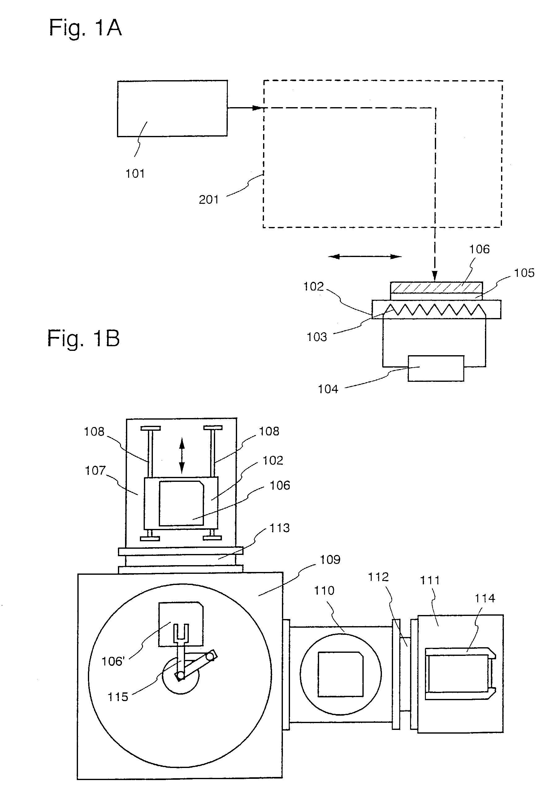
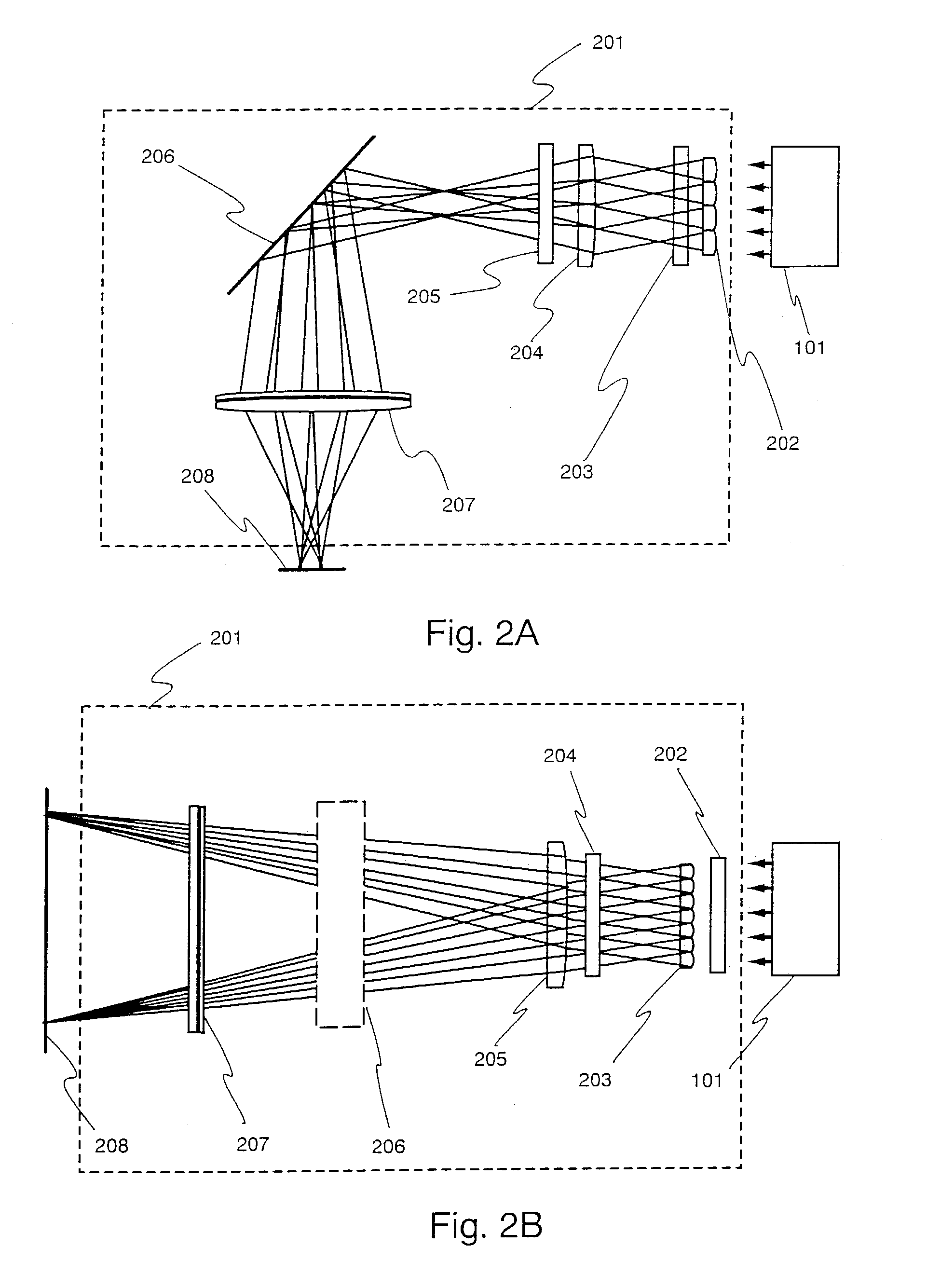
[0076]An embodiment mode of the present invention is explained. FIG. 1A is a diagram showing the structure of a laser apparatus. The laser apparatus has a laser 101, an optical system 201 for converting laser light from the laser 101 as an emission source into a linear shape, and a stage 102 which is fixed to a transparent substrate. A heater 103 and a heater controller 104 are provided on the stage 102, and the substrate can be maintained at a temperature in a range from room temperature to 550° C. Further, a reflecting body 105 is formed on the stage 102, and a substrate 106 on which an amorphous semiconductor film is formed is arranged on top of the reflecting body 105.

[0077]A method of maintaining the substrate 106 in the laser apparatus having the structure of FIG. 1A is explained next using FIG. 1B. The substrate 106 maintained on the stage 102 is placed in a reaction chamber 107, and linear shape laser light from the laser 101 as the emission source is irradiated. The inside ...

embodiment mode 2

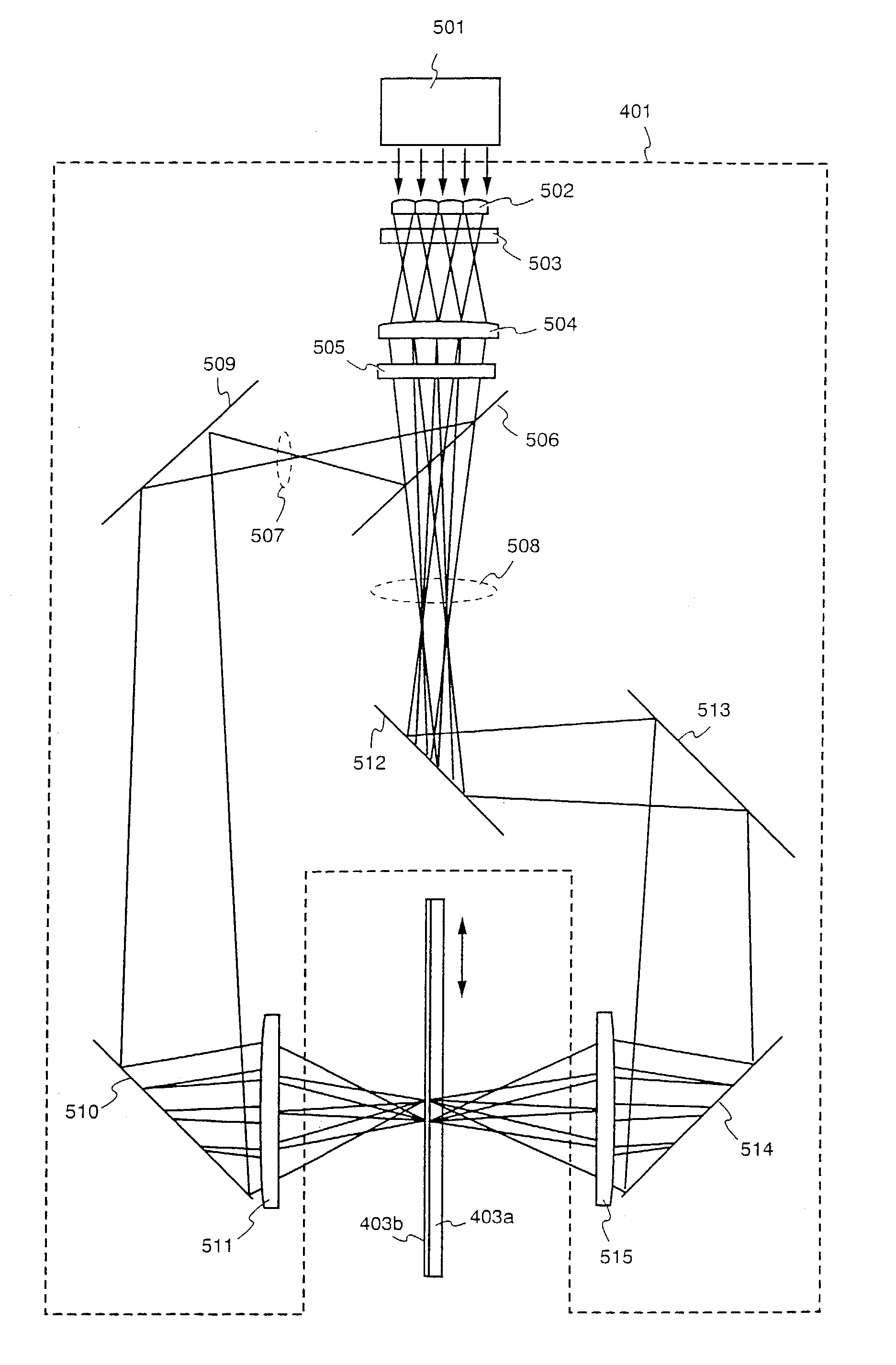
[0092]An implementation which differs from that of embodiment mode 1 is explained in embodiment mode 2. A reflecting body similar to that of embodiment mode 1 is not used in embodiment mode 2, and an example of irradiating dual stream laser light, separated midstream in an optical system, on the top surface and the bottom surface of an amorphous semiconductor film is shown.

[0093]FIG. 4A is a diagram showing the structure of the laser apparatus of embodiment mode 2. The basic structure is similar to that of the laser apparatus of FIG. 1 explained by embodiment mode 1, and therefore symbols are changed for differing portions to be explained.

[0094]The laser apparatus has the laser 101, an optical system 401 which transforms laser light from the laser 101 as the emission source into a linear shape, and separates the light into dual streams, and a transparent stage 402 for fixing a transparent substrate. Further, a substrate 403a is placed on the stage 402, and an amorphous semiconductor...

embodiment 1

[0106]An example is shown in embodiment 1 of performing crystallization of an amorphous silicon film with the structure shown in embodiment mode 1. FIG. 3 is used for the explanation.

[0107]A 1.1 mm thick quartz substrate is used as the substrate 301 in embodiment 1, a 200 nm thick silicon oxynitride film (SiON film) is used as the insulating film 302, and an amorphous silicon film is used as the amorphous semiconductor film 303. The SiON film 302 and the amorphous silicon film 303 are formed by using plasma CVD at this point.

[0108]In embodiment 1, at first SiH4 is introduced into the reaction chamber at 4 SCCM, and N2O is introduced at 400 SCCM. The SiON film 302 is formed with a film deposition temperature of 400° C., a reaction pressure of 30 Pa, a discharge power density of 0.41 W / cm2, and a discharge frequency of 60 MHz. Next, SiH4 is introduced into the reaction chamber at 100 SCCM, and the amorphous silicon film 303 is formed with a film deposition temperature of 300° C., a re...


PUM


Abstract

A laser annealing method for obtaining a crystalline semiconductor film having a large grain size is provided. Laser light is irradiated to the top surface and the bottom surface of an amorphous semiconductor film when crystallizing the amorphous semiconductor film by laser light irradiation. Furthermore, a relationship of 0<(I0′/I0)<1, or 1<(I0′/I0) is achieved for the ratio (I0/I0′) between the effective energy strength of the laser light when irradiated to the top surface (I0) and the effective energy strength of the laser light when irradiated to the bottom surface (I0′).

Description

BACKGROUND OF THE INVENTION[0001]1. Field of the Invention[0002]The present invention relates to a method of annealing a semiconductor film using laser light (hereafter referred to as laser annealing), and to a laser apparatus for performing laser annealing (an apparatus containing a laser and an optical system for guiding the laser light output from the laser to a processing piece. In addition, the present invention relates to a semiconductor device formed by using that type of laser annealing method, and to a method of manufacturing the semiconductor device.[0003]2. Description of the Related Art[0004]The development of thin film transistors (hereafter referred to as TFTs) has been advancing in recent years, and TFTs using a polycrystalline silicon film (polysilicon film) as a crystalline semiconductor film have been in the spotlight. In particular, the TFTs are used as elements forming a driver circuit for controlling a pixel, or an element which switches the pixel, in a liquid c...

Claims


Application Information

Patent Timeline
Patent Type & Authority Patents(United States)
IPC IPC(8): H01L21/26H01L21/20H01L21/336H01L21/77H01L21/84H01L27/12H01L29/786
CPCH01L21/2026H01L27/12H01L29/66757H01L27/1285H01L29/78624H01L29/78633H01L29/78675H01L29/78621H01L21/0262H01L21/02686H01L21/02422H01L21/02488H01L21/02678H01L21/02532H01L21/0242H01L21/02595H01L21/02691H01L21/02675
Inventor KASAHARA, KENJIKAWASAKI, RITSUKOOHTANI, HISASHIYAMAZAKI, SHUNPEI
Owner SEMICON ENERGY LAB CO LTD
Why Eureka
Try Eureka