Methods and apparatus for inducing stress in a semiconductor device

a technology of inducing stress and semiconductor devices, applied in semiconductor devices, transducer details, electrical transducers, etc., can solve the problems of reducing the affecting the power consumption and switching performance of the device, and reducing the gate length, so as to facilitate the induced stress effect, improve the carrier mobility, and induce stress

Inactive Publication Date: 2008-03-04
TEXAS INSTR INC
View PDF29 Cites 0 Cited by
  • Summary
  • Abstract
  • Description
  • Claims
  • Application Information

AI Technical Summary

Benefits of technology

[0010]Another aspect of the invention provides a semiconductor device, having first and second regions in a substrate. The first region is implanted so as to induce stress in the second region, and an electrical device or a portion thereof is provided in the second region. The first region may be located beneath at least a portion of the second region, or be near the second region in order to facilitate the induced stress effect therein. The electrical device may be, for example, a transistor with a source / drain region or a channel region formed within the second region, and the first region may be implanted with carbon, germanium, and / or oxygen so as to induce stress in the second region. Yet another aspect of the invention provides a method of improving carrier mobility in a channel region of a MOSFET device, which involves implanting a first region in a substrate so as to induce stress in a second region in the substrate, and forming at least a portion of the channel in the second region of the substrate.

Problems solved by technology
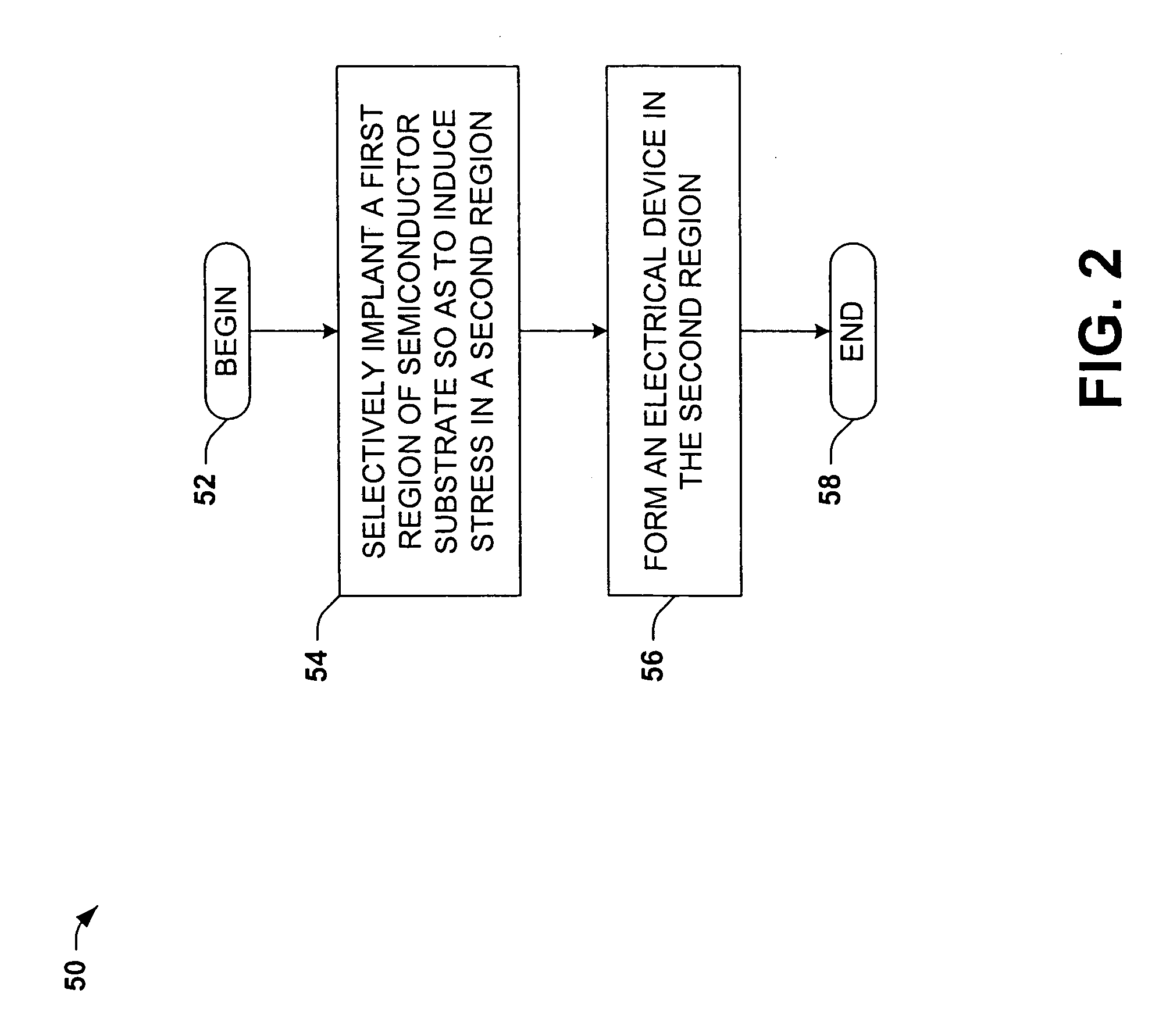
The carrier mobility in a MOSFET device can have a significant impact on power consumption and switching performance.
However, reducing the gate dielectric thickness results in an increase in gate tunneling current, which in turn degrades the performance of the device by increasing off state leakage.
In addition, decreasing gate length generally requires more advanced and expensive lithography technology.
However, such buried silicon / germanium channel layer devices have shortcomings, including increased alloy scattering in the channel region that degrades electron mobility, a lack of favorable conduction band offset which mitigates the enhancement of electron mobility and the need for large germanium concentrations to produce strain and thus enhanced mobility.
Furthermore, such additional alloy layers and silicon layers are costly, adding further processing steps to the device manufacturing procedure.

Method used


Image

  • Methods and apparatus for inducing stress in a semiconductor device
  • Methods and apparatus for inducing stress in a semiconductor device
  • Methods and apparatus for inducing stress in a semiconductor device

Examples


Embodiment Construction

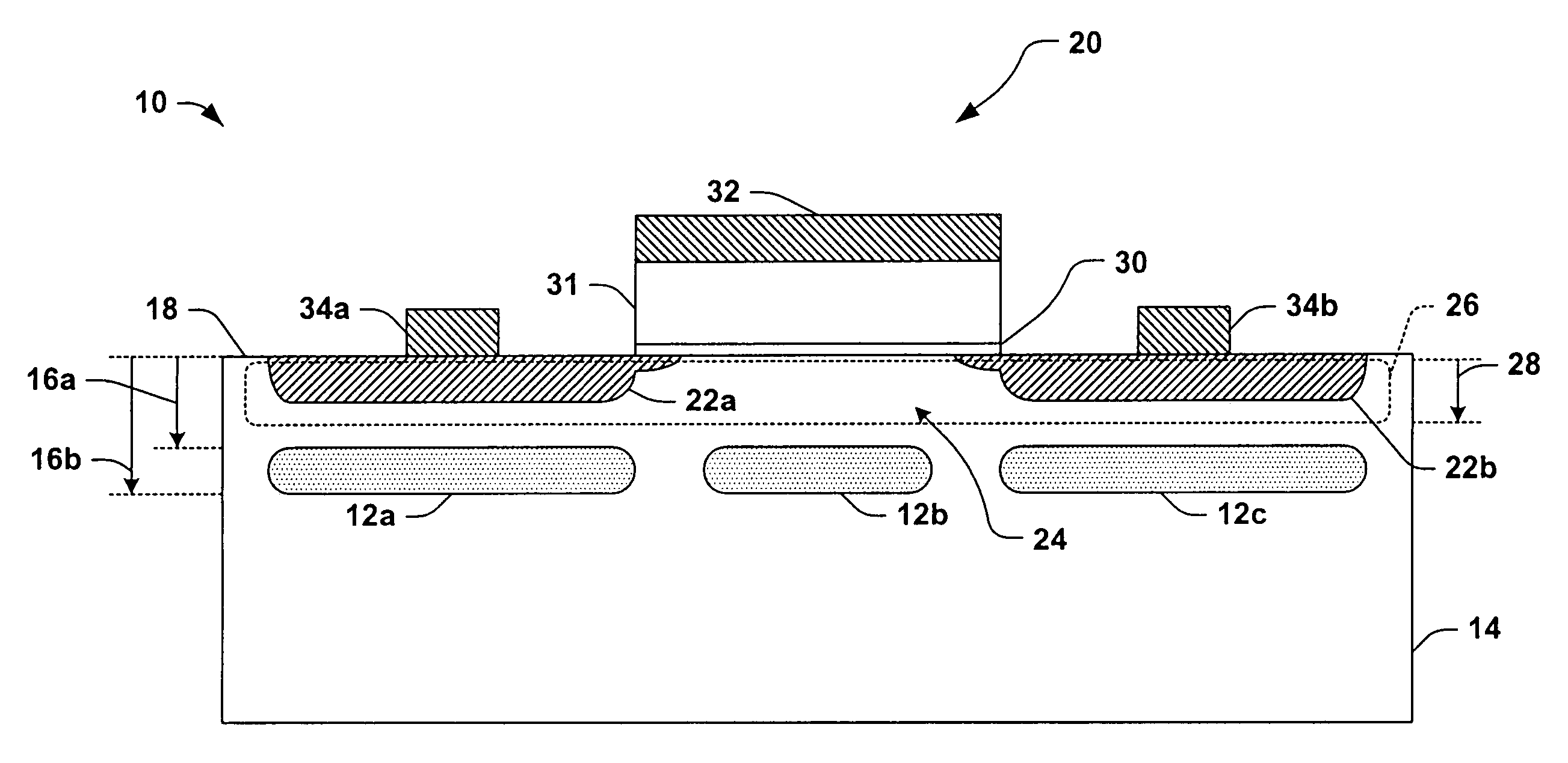
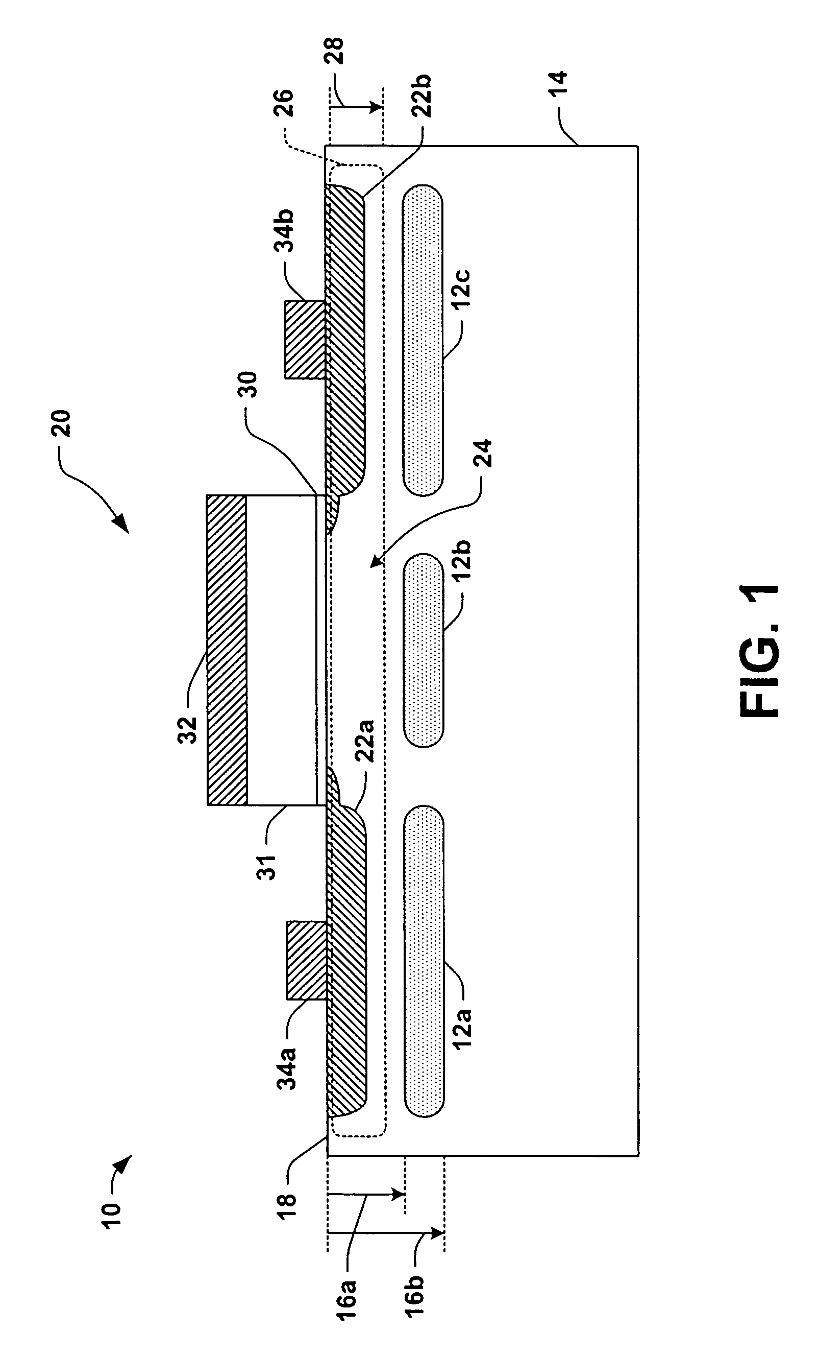
[0019]The present invention will now be described with reference to the attached drawings, wherein like reference numerals are used to refer to like elements throughout. The invention relates to methods and structures for influencing stress in an electrical region of a semiconductor device, by which one or more operational performance characteristics of the device may be improved. In the illustrated examples which follow, several implementations of the invention are shown and described which operate to improve carrier mobility in MOSFET type transistors. However, it will be appreciated that the various aspects of the invention may be employed to improve or modify other characteristics of semiconductor devices apart from carrier mobility, as well as in association with devices other than MOSFET transistors. For example, alternatively or in combination with affecting carrier mobility, the present invention may be advantageously employed in improving diffusion behavior, silicidation, a...


PUM


Abstract

Methods and apparatus are disclosed for selectively inducing stress in a semiconductor device, wherein a first region of a substrate is implanted so as to induce stress in a second region. An electrical device is formed at least partially in the second region, wherein the induced stress therein may improve one or more operational characteristics of the device, such as channel region carrier mobility.

Description

[0001]This application is a divisional of application Ser. No. 10 / 020,111, filed Dec. 14, 2001 now U.S. Pat. No. 6,806,151.FIELD OF INVENTION[0002]The present invention relates generally to semiconductor devices and more particularly to methods and apparatus for fabricating semiconductor devices using implantation to induce stress in an electrical device.BACKGROUND OF THE INVENTION[0003]Many conventional semiconductor devices include metal-oxide-semiconductor field-effect transistor (MOSFET) and other transistor devices to perform a variety of functions, such as switching, amplification, and the like. As required switching speeds increase and as operating voltages levels decrease in semiconductor products, the performance of transistors within such products needs to be correspondingly improved. For instance, switching speed requirements of MOSFETs and other transistors continue to increase in order to facilitate faster and improved product performance. Moreover, as such devices incr...

Claims


Application Information

Patent Timeline
Patent Type & Authority Patents(United States)
IPC IPC(8): H01L21/336H01L21/265H01L21/762H01L29/78
CPCH01L21/76283H01L29/78H01L29/7842H01L29/7848H01L21/26506H01L29/7833H01L29/1083
Inventor WASSHUBER, CHRISTOPHJOYNER, KEITH A.
Owner TEXAS INSTR INC
Why Eureka
Try Eureka