Method to fabricate patterned strain-relaxed SiGe epitaxial with threading dislocation density control

a technology of density control and strainrelaxed sige, which is applied in the direction of chemically reactive gas growth process, polycrystalline material growth, crystal growth process, etc., can solve the problems of random threading dislocation, concentration of threading dislocation of active areas in non-active areas

Inactive Publication Date: 2008-03-11
IND TECH RES INST
View PDF5 Cites 4 Cited by
  • Summary
  • Abstract
  • Description
  • Claims
  • Application Information

AI Technical Summary

Benefits of technology

[0015]According to an aspect of the invention, an advantage of the invention provides a better strain-relaxed SiGe epitaxial layer to improve the carrier shift mobility of the channel of the strained silicon. The conventional method to deposit a gradual SiGe epitaxial layer results in threading dislocation at random. However, employing ion implanting to define the active area and the non-active area results in concentration of the threading dislocation of the active areas in the non-active area. Therefore, the method according to the aspect of the invention is helpful for the performance enhancement of semiconductor devices.

Problems solved by technology

The conventional method to deposit a gradual SiGe epitaxial layer results in threading dislocation at random.
However, employing ion implanting to define the active area and the non-active area results in concentration of the threading dislocation of the active areas in the non-active area.

Method used


Image

  • Method to fabricate patterned strain-relaxed SiGe epitaxial with threading dislocation density control
  • Method to fabricate patterned strain-relaxed SiGe epitaxial with threading dislocation density control
  • Method to fabricate patterned strain-relaxed SiGe epitaxial with threading dislocation density control

Examples


Embodiment Construction

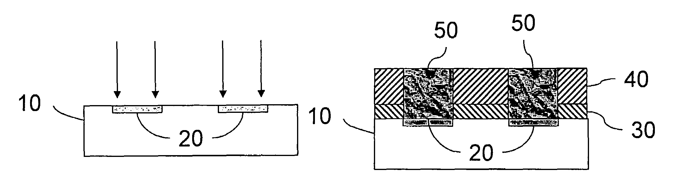
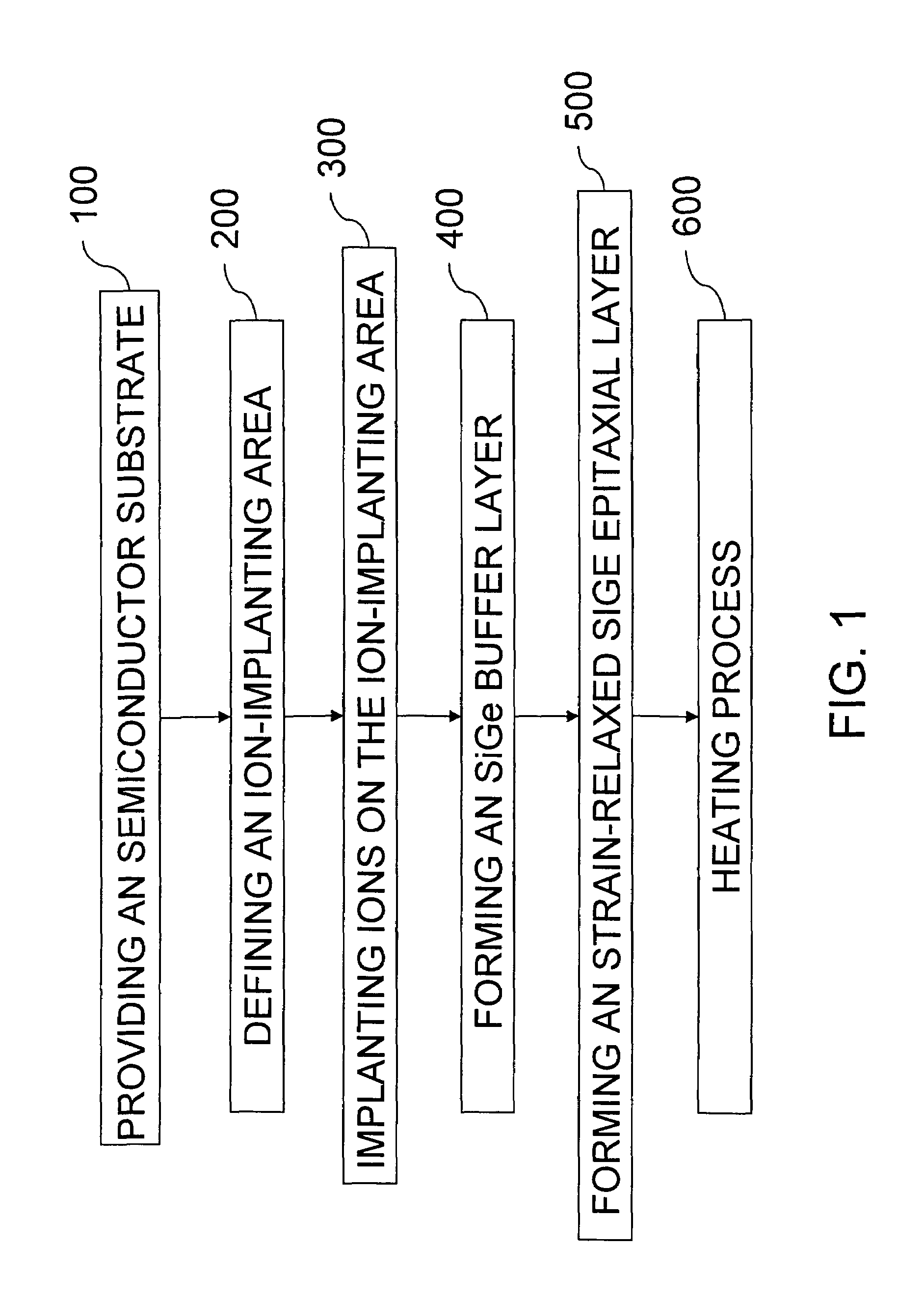
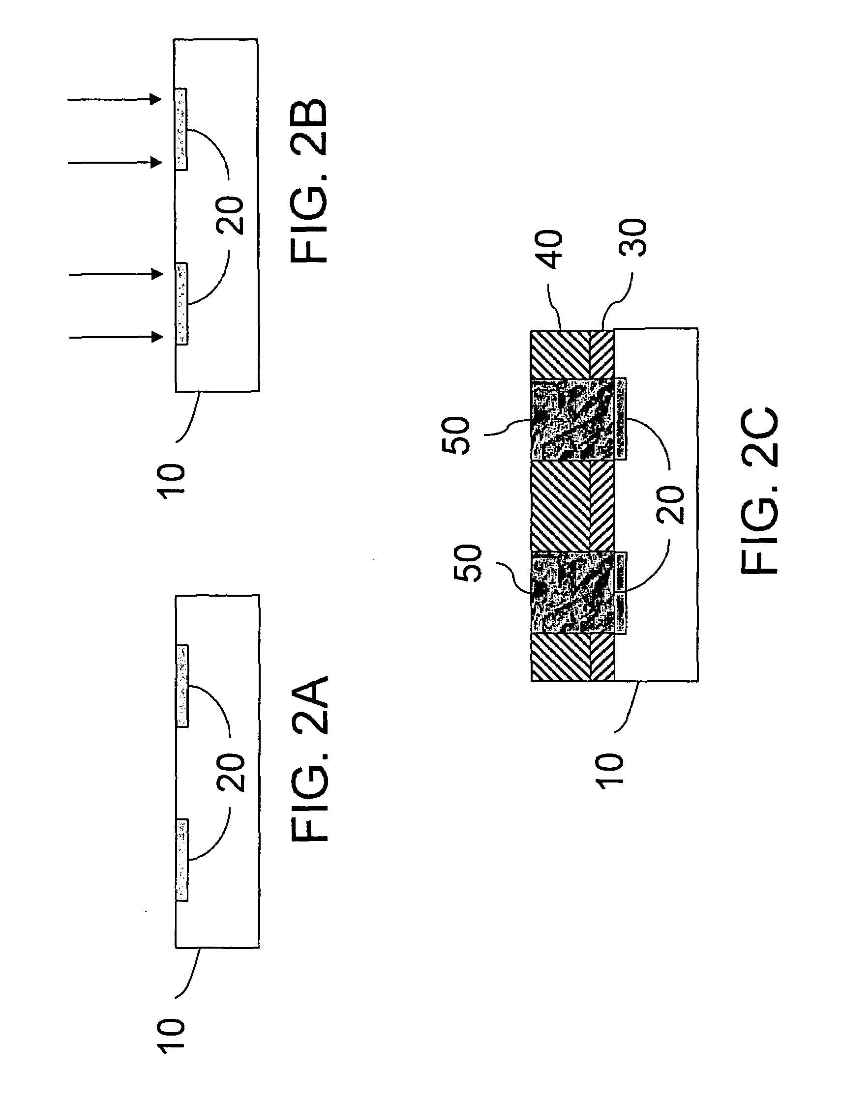
[0022]Refer to FIG. 1, illustrating the fabricating process of patterned strain-relaxed SiGe epitaxy with threading dislocation density control according to the version of the invention. Steps of the process can be performed in different sequences, or some of the steps can be omitted, or performed simultaneously. The sequence and number of steps are not particularly limited to those described in the following embodiments.

[0023]The ion-implanting area is defined through using a photo mask. Then, a gradual SiGe epitaxial layer (content around 0˜20%) is deposited by super vacuum chemical vapor deposition and an appropriate heating process. The non ion-implanting areas are used to fabricate semiconductor components.

[0024]In the beginning, a semiconductor substrate is provided (step 100). Then a photo mask is employed to define an ion-implanting area (step 200). The ion-implanting area is a non active area while the non ion-implanting area is an active area. Then, an ion implanting proce...


PUM

PropertyMeasurementUnit
dislocation densityaaaaaaaaaa
areaaaaaaaaaaa
semiconductoraaaaaaaaaa

Abstract

A method to fabricate patterned strain-relaxed SiGe epitaxial with threading dislocation density control is provided. An ion-implanting area is first defined on a silicon substrate, and then proceeds ion-implanting. Finally, a buffer layer and a SiGe epitaxial layer are deposited. According to the disclosure, an active area and a non-active area are defined through ion-implanting. Therefore, the threading dislocation occurring in the active area concentrates in the non-active area, and the density of the threading dislocation is lowered. Furthermore, the performance of the semiconductor is also enhanced.

Description

[0001]This Non-provisional application claims priority under 35 U.S.C. § 119(a) on Patent Application No(s). 093102861 filed in Taiwan on Feb. 6, 2004, the entire contents of which are hereby incorporated by reference.BACKGROUND OF THE INVENTION[0002]1. Field of Invention[0003]The present invention relates to a method to fabricate strain-relaxed SiGe layers, and more particularly to a method to fabricate a patterned strain-relaxed SiGe epitaxy with threading dislocation density control.[0004]2. Related Art[0005]The semiconductor and integrated circuit technology has been developed to be compact with high operation speed in recent years. How to increase the operation speed of the semiconductor device and lower power consumption constitutes an important issue in the very large scale integration (VLSI) field.[0006]Researches on SiGe material have shown that deposition of a strained Si after depositing a strain-relaxed SiGe layer on a silicon substrate, increases electron shift mobility...

Claims


Application Information

Patent Timeline
Patent Type & Authority Patents(United States)
IPC IPC(8): H01L21/20C30B23/04C30B25/04C30B29/52C30B31/22H01L21/324H01L29/10
CPCC30B23/04C30B25/04C30B29/52C30B31/22H01L21/02381H01L21/0245H01L29/1054H01L21/0251H01L21/02532H01L21/02658H01L21/324H01L21/02502H01L21/02639
Inventor TSENG, YANG-TAICHEN, PANG-SHIULU, SHIN-CHI
Owner IND TECH RES INST
Why Eureka
Try Eureka