

Method of preparing gate dielectric film of SiC-based MOS device
A technology of MOS devices and gate dielectrics, applied in the manufacture of semiconductor/solid-state devices, electrical components, circuits, etc., can solve the problem of low carrier mobility, reduce the interface state density, and improve the channel carrier mobility. Effect
- Summary
- Abstract
- Description
- Claims
- Application Information
AI Technical Summary
Problems solved by technology
Method used
Image

Examples
Embodiment 1
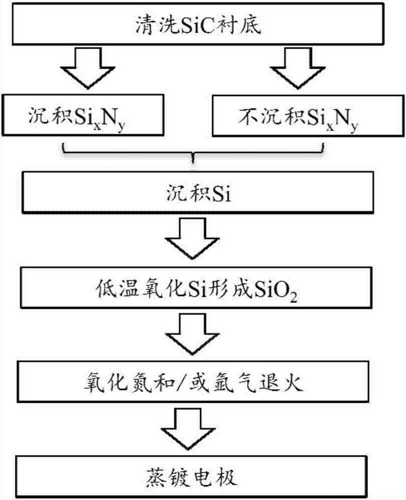
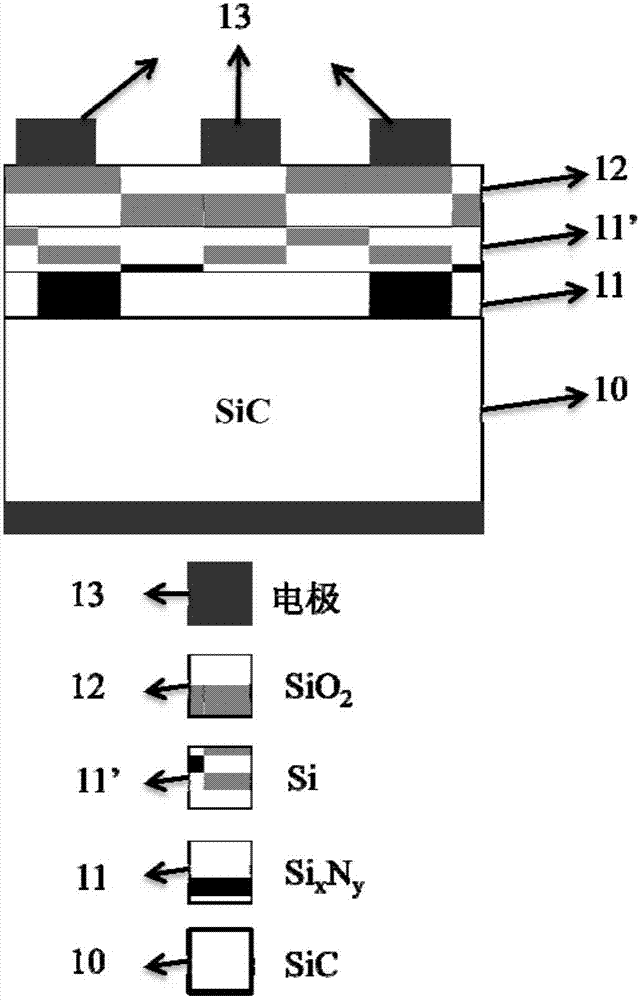
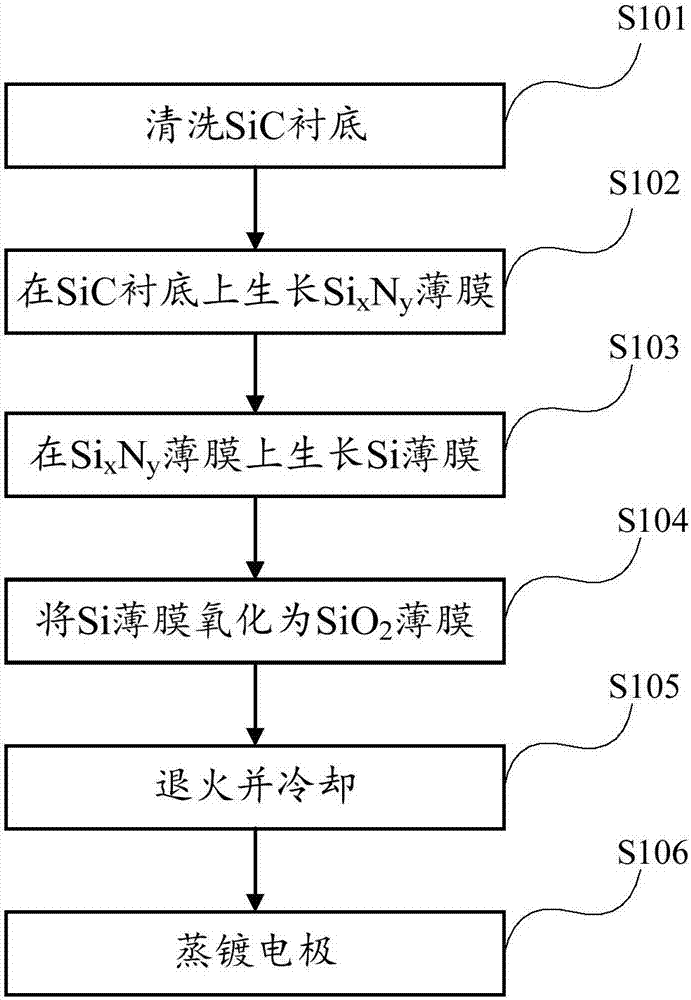
[0049] figure 2 It is a flow chart of the method for preparing a SiC-based MOS device gate dielectric film related to Embodiment 1. This embodiment involves Si x N y / SiO 2 gate dielectric layer.
[0050] First, step S101 is performed to clean the SiC substrate. In this embodiment, a 4H-SiC substrate sample is used, and a standard cleaning is performed on the 4H-SiC substrate sample.
[0051] a. Ultrasonic cleaning three times with toluene, acetone and ethanol in sequence, and then rinsed with deionized water.
[0052] b. Soak the rinsed substrate in diluted hydrofluoric acid (hydrogen fluoride: deionized water = 1:3 by volume) for 1 min.
[0053] c. Boil the substrate soaked in hydrofluoric acid in concentrated sulfuric acid for 10 minutes.
[0054] d. Boil the substrate boiled in concentrated sulfuric acid with No. 1 solution and No. 2 solution for 15 minutes, rinse it with deionized water, and dry it with nitrogen gas for use. The No. 1 liquid is a mixture of ammonia...
Embodiment 2
[0062] image 3 It is a flow chart of the method for preparing a SiC-based MOS device gate dielectric film related to the second embodiment, and this embodiment involves SiO 2 gate dielectric layer.
[0063] First, step S201 is performed to clean the SiC substrate. In this embodiment, a 4H-SiC substrate sample is used, and a standard cleaning is performed on the 4H-SiC substrate sample.
[0064] a. Ultrasonic cleaning three times with toluene, acetone and ethanol in sequence, and then rinsed with deionized water.
[0065] b. Soak the rinsed substrate in diluted hydrofluoric acid (hydrogen fluoride: deionized water = 1:3 by volume) for 1 min.
[0066] c. Boil the substrate soaked in hydrofluoric acid in concentrated sulfuric acid for 10 minutes.
[0067] d. Boil the substrate boiled in concentrated sulfuric acid with No. 1 solution and No. 2 solution for 15 minutes, rinse it with deionized water, and dry it with nitrogen gas for use. The No. 1 liquid is a mixture of ammoni...
PUM
| Property | Measurement | Unit |
|---|---|---|
| Thickness | aaaaa | aaaaa |
| Thickness | aaaaa | aaaaa |
| Thickness | aaaaa | aaaaa |
Abstract
Description
Claims
Application Information