
Method to reduce charge buildup during high aspect ratio contact etch

a high aspect ratio, contact etching technology, applied in the direction of basic electric elements, electrical equipment, semiconductor devices, etc., can solve the problems of etching stop, charge accumulation, build-up damage, etc., to prevent the twisting of the contact hole, and reduce the charge build-up

Active Publication Date: 2008-03-18
MICRON TECH INC
View PDF5 Cites 6 Cited by
  • Summary
  • Abstract
  • Description
  • Claims
  • Application Information

AI Technical Summary

Benefits of technology

The conductive carbon chain polymers reduce charge buildup, preventing contact hole twisting and ensuring proper alignment, while maintaining the etch component's functionality without shutting it off.

Problems solved by technology

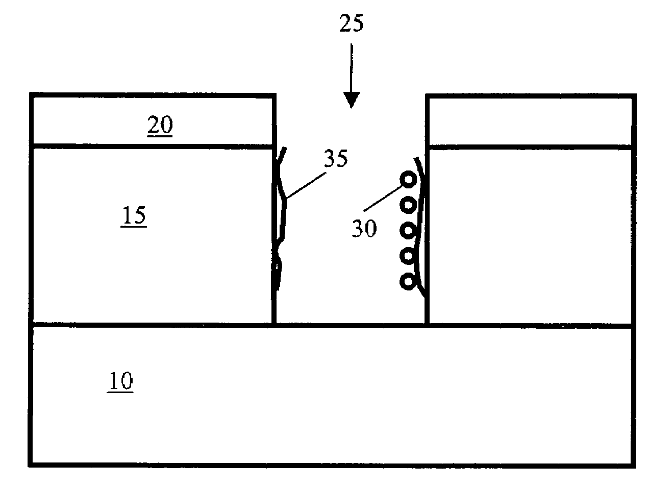
During plasma etching, plasma electrons, due to their random thermal motion, tend to impinge on the sidewalls near the top of the contact hole causing charge accumulation.
Charge accumulation is one of the main causes of charge build-up damage, etching stop, as well as micro-loading effects.
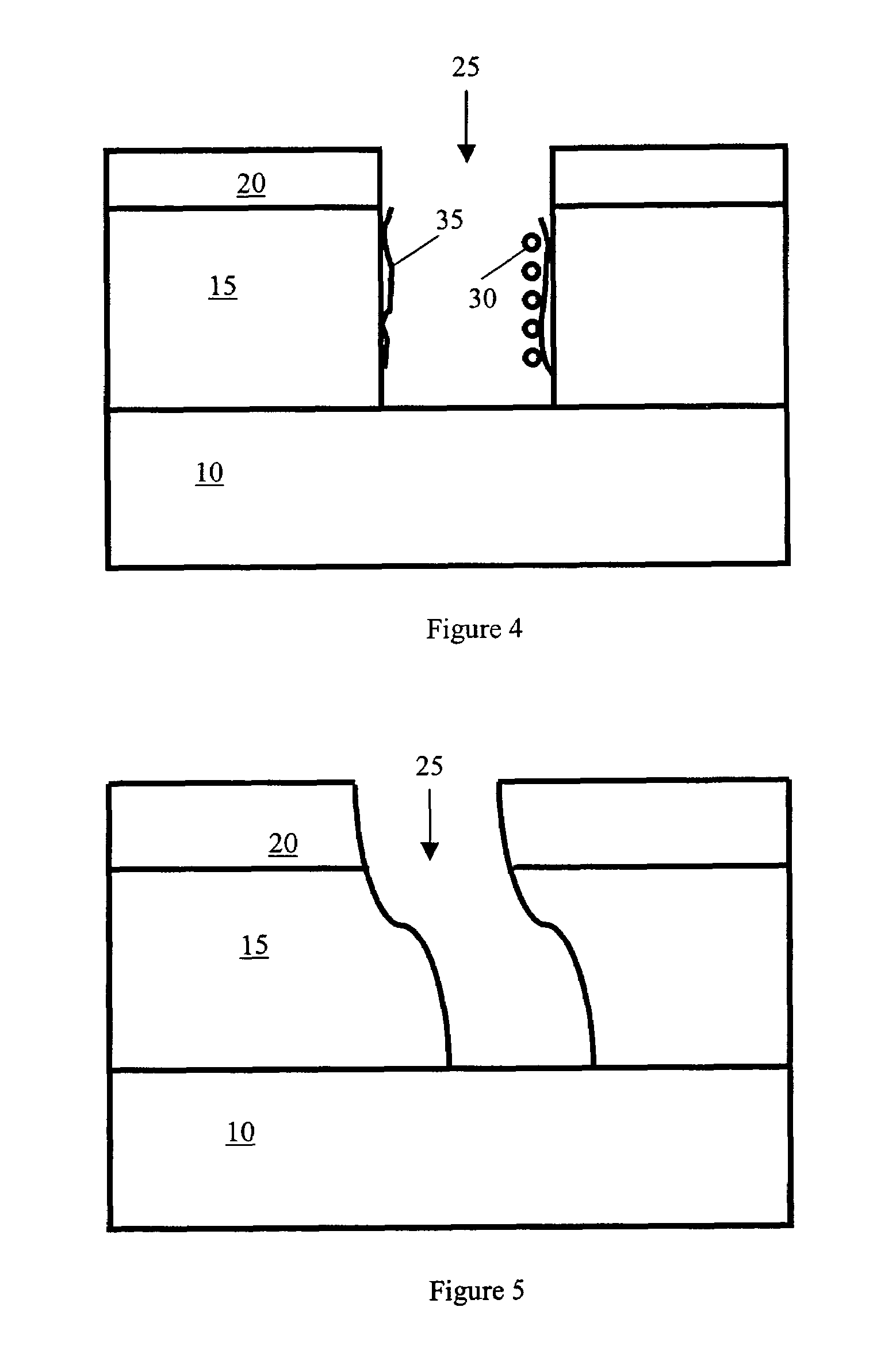
Conductivity of the sidewalls in the contact holes increases during the etching processes resulting in carbon chain polymer buildup along the sidewalls of the contact hole.
Over the course of the etch process, the bottom of the contact hole charges positively while the sidewalls charge negatively, thereby creating undesired local electric fields within the contact hole.
This, in turn, results in the contact hole twisting during its formation and becoming non-vertical.
Further, sidewall charging may also lead to complete etch stoppage in HARC contact holes.
Another related issue associated with the charge buildup along the sidewalls is that the contact hole misses the active area landing region in the underlying substrate due to the twisting of the contact hole during its formation.

Method used


Image

  • Method to reduce charge buildup during high aspect ratio contact etch
  • Method to reduce charge buildup during high aspect ratio contact etch
  • Method to reduce charge buildup during high aspect ratio contact etch

Examples


Embodiment Construction

[0020]In the following detailed description of the preferred embodiments, reference is made to the accompanying drawings that form a part hereof, and in which are shown by way of illustration, and not by way of limitation, specific preferred embodiments in which the invention may be practiced. It is to be understood that other embodiments may be utilized and that logical, mechanical and electrical changes may be made without departing from the spirit and scope of the present invention.

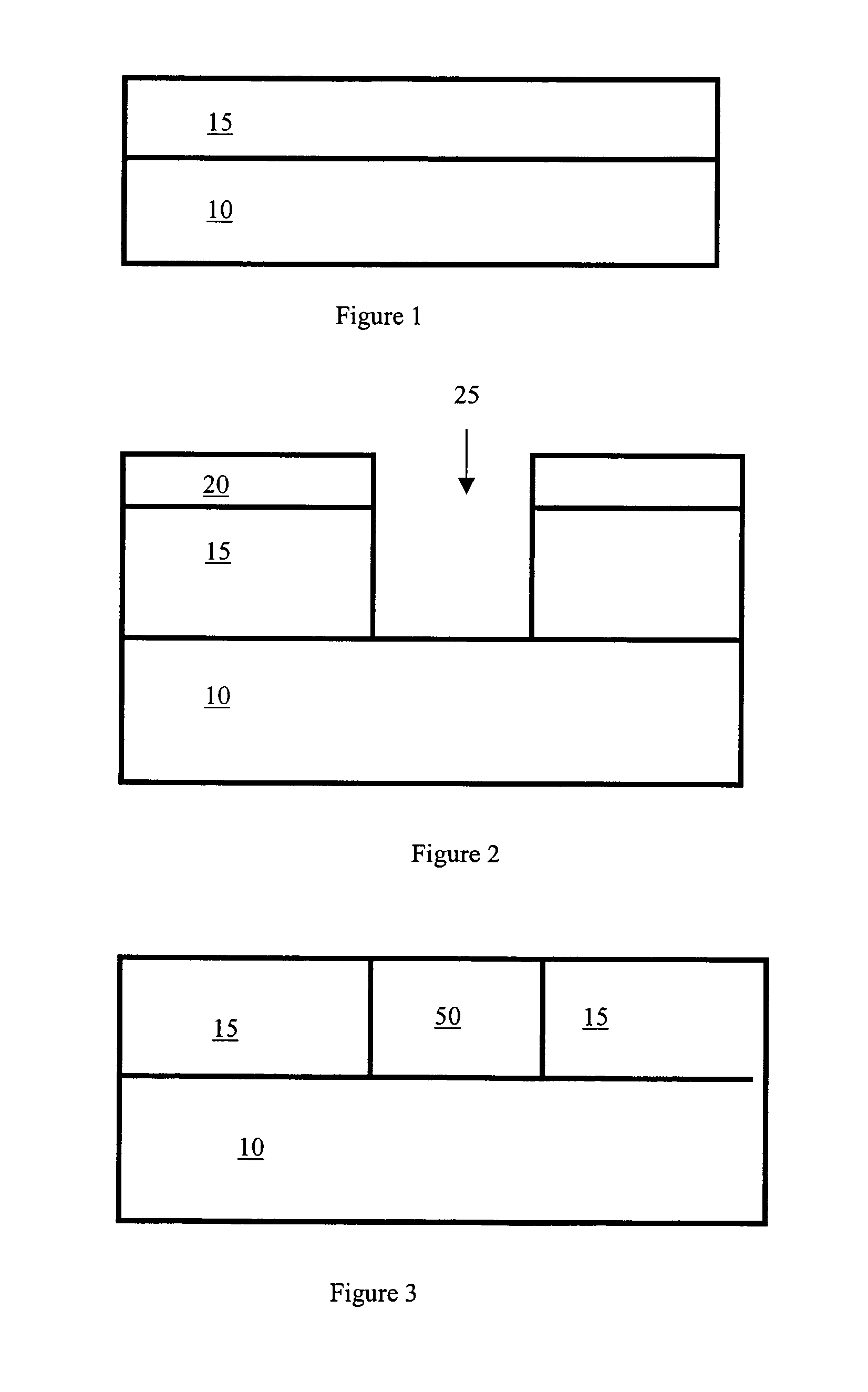
[0021]FIG. 1 illustrates a partially completed semiconductor device. The devices comprises a substrate layer 10. An oxide layer 15 is deposited on top of the substrate layer 10. The substrate layer 10 is typically comprised of silicon, silicon oxide or any other suitable material known in the art. The oxide layer 15 can be comprised of borophosphosilicate (BPSG), tetraethylorthosilicate (TEOS), phosphorous-doped silicate glass (PSG) or any other suitable oxide material.

[0022]FIG. 2 illustrates the part...


PUM


Abstract

A method of high aspect ratio contact etching a substantially vertical contact hole in an oxide layer using a hard photoresist mask is described. The oxide layer is deposited on an underlying substrate. A plasma etching gas is formed from a carbon source gas. Dopants are mixed into the gas. The doped plasma etching gas etches a substantially vertical contact hole through the oxide layer by doping carbon chain polymers formed along the sidewalls of the contact holes during the etching process into a conductive state. The conductive state of the carbon chain polymers reduces the charge buildup along sidewalls to prevent twisting of the contact holes by bleeding off the charge and ensuring proper alignment with active area landing regions. The etching stops at the underlying substrate.

Description

BACKGROUND OF THE INVENTION[0001]The present invention generally relates to High Aspect Ratio Contact trench etching and, in particular, relates to the reduction of charge buildup along the trench sidewalls during High Aspect Ratio Contact trench etching.[0002]Successful construction of nano- and microstructures requires reliable and reproducible methods of production. One such nano- or microstructure is a contact hole, or trench. Contact hole structures are generally fabricated using wet (crystal anisotrophy) or dry plasma (ion-bombardment anisotrophy) etching. One example of a contact hole formed by dry plasma etching is shaped by etching through an oxide layer overlaying a silicon substrate using a hard photoresist mask deposited on top of the oxide layer, wherein the etching substantially stops on the underlying substrate layer. Contact holes have a diameter, also known as width, and a depth. The diameter is referred to as the feature size and tends to decrease with increasing c...

Claims


Application Information

Patent Timeline
Patent Type & Authority Patents(United States)
IPC IPC(8): H01L21/4763
CPCH01L21/31116H01L21/76802Y10S438/906
Inventor SANDHU, GURTEJ S.HINEMAN, MAX F.STECKERT, DANIEL A.BAI, JINGYITRAPP, SHANE J.SCHROCK, TONY
Owner MICRON TECH INC
Learn More