Method and apparatus for optimizing a logic network in a digital circuit

a logic network and digital circuit technology, applied in the field of logic synthesis, can solve the problems of long gate delay, inability to identify and remove redundant logic, and increase the density and complexity of integrated circuits, and achieve the effect of efficiently optimizing, efficiently optimizing, and efficiently optimizing the first logic network

Active Publication Date: 2008-03-18
SYNOPSYS INC
View PDF21 Cites 9 Cited by
  • Summary
  • Abstract
  • Description
  • Claims
  • Application Information

AI Technical Summary

Benefits of technology

[0011]One embodiment of the present invention provides a system that optimizes a logic network. During operation, the system receives a first logic network which defines a logical function, wherein the first logic network cannot be efficiently optimized by directly using an optimization process that preserves the logical function. Next, the system creates an intermediate logic network based on the first logic network, wherein the intermediate logic network defines an intermediate logical function which is different from the logical function, wherein the intermediate logic network can be efficiently optimized using the optimization process. The system then optimizes the intermediate logic network using the optimization process to create an optimized intermediate logic network. Next, the system creates an optimized first logic network based on the optimized intermediate logic network. In this way, the system indirectly uses the optimization process to efficiently optimize the first logic network.
[0015]In a variation on this embodiment, the system optimizes the intermediate logic network using the optimization process by: minimizing timing delay by reducing logic levels and sharing common logic. Specifically, the system shares common logic by first identifying common logic in cases where two logic cones are found to have the same set of inputs, but different outputs. If common logic is identified, the system removes one of the logic cones.

Problems solved by technology

These advances can be largely attributed to the exponential increase in the density and complexity of integrated circuits.
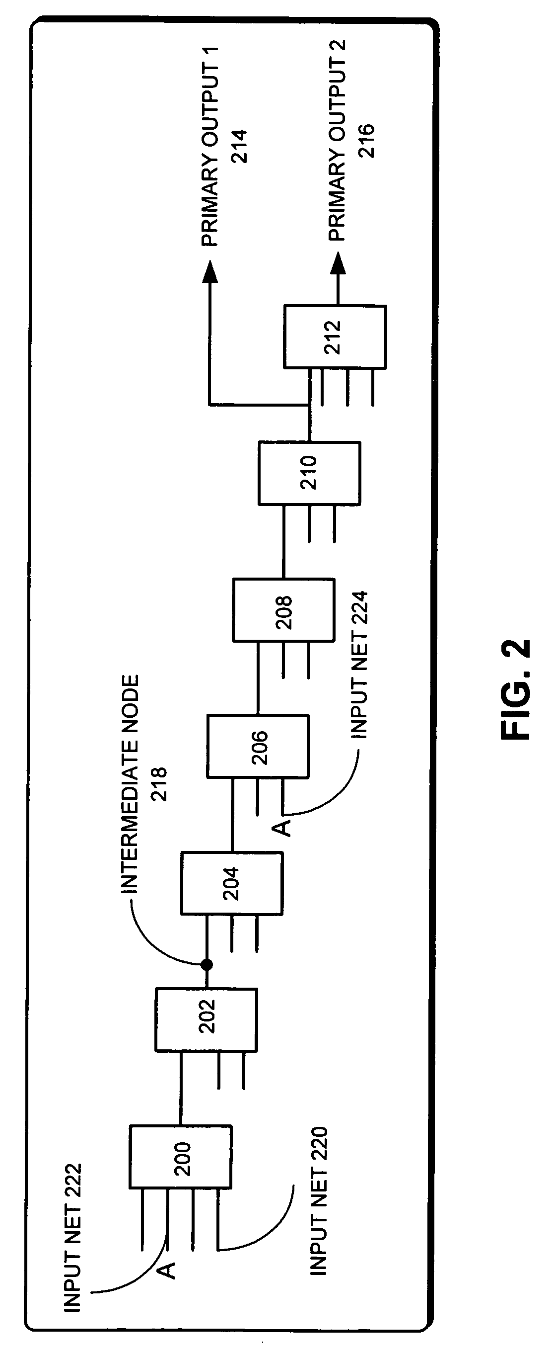
For the previous example, a hardware implementation of the CRCn system typically uses a cascade XOR gate structure, which is also referred to as an “XOR-tree.” Note that for a system that implements CRCn there can be as many as n gate levels in the cascade structure, which may result in long gate delays.
Furthermore, the cascade structure can miss redundant logic identification and removal in the XOR-tree and common logic sharing among the XOR-trees.
The first method can reduce gate delays by reducing gate levels, but can miss the common logic sharing.
The second method can identify some of the logic sharing, but can not minimize the gate delays, and can not identify all the common logic sharing.
The XOR-tree optimization has been a difficult synthesis problem for a very long time.
Unfortunately, so far no effective synthesis tool has been developed which can optimize an XOR logic network to minimize delay and chip area at the same time.
Besides delay and speed problems, there are further problems.
For example, it is also difficult to identify and remove redundant logic.

Method used


Image

  • Method and apparatus for optimizing a logic network in a digital circuit
  • Method and apparatus for optimizing a logic network in a digital circuit
  • Method and apparatus for optimizing a logic network in a digital circuit

Examples


Embodiment Construction

Integrated Circuit Design Flow

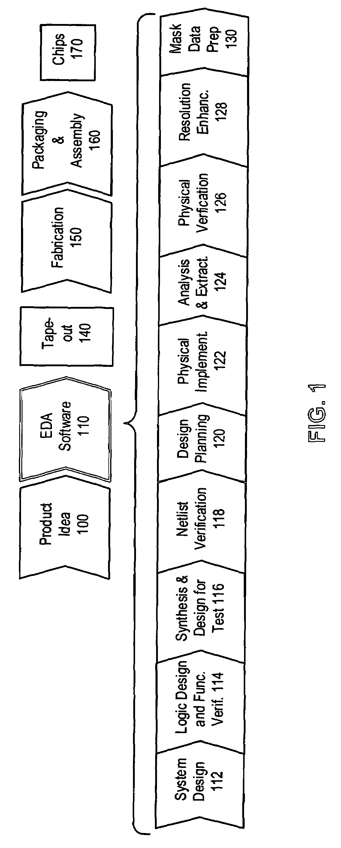
[0028]FIG. 1 illustrates an exemplary integrated circuit design flow in accordance with an embodiment of the present invention.

[0029]The process starts with the product idea (step 100) which is realized using an EDA software design process (step 110). When the design is finalized, it can be taped-out (event 140). After tape out, the fabrication process (step 150) and packaging and assembly processes (step 160) are performed which ultimately result in finished chips (result 170).

[0030]The EDA software design process (step 110), in turn, comprises steps 112-130, which are described below. Note that the design flow description is for illustration purposes only. Specifically, this description is not meant to limit the present invention. For example, an actual integrated circuit design may require the designer to perform the design steps in a different sequence than the sequence described below. The following text provides a brief description of the steps in...


PUM


Abstract

One embodiment of the present invention provides a system that optimizes a logic network. During operation, the system receives a first logic network which defines a logical function, wherein the first logic network cannot be efficiently optimized by directly using an optimization process that preserves the logical function. Next, the system creates an intermediate logic network based on the first logic network, wherein the intermediate logic network defines an intermediate logical function which is different from the logical function, wherein the intermediate logic network can be efficiently optimized using the optimization process. The system then optimizes the intermediate logic network using the optimization process to create an optimized intermediate logic network. Next, the system creates an optimized first logic network based on the optimized intermediate logic network. In this way, the system indirectly uses the optimization process to efficiently optimize the first logic network.

Description

BACKGROUND[0001]1. Field of the Invention[0002]The present invention relates to techniques for logic synthesis. More specifically, the present invention relates to a method and an apparatus for optimizing a logic network in a digital circuit.[0003]2. Related Art[0004]Rapid advances in computing technology presently make it possible to perform trillions of operations each second on data sets that are sometimes as large as a trillion bytes. These advances can be largely attributed to the exponential increase in the density and complexity of integrated circuits. High-density integrated circuits, such as a CPU chip, can have logic gate densities up to 500,000 gates per mm2, which makes it possible to implement many complex logical functions.[0005]A logical function is performed by a group of interconnected logic gates, which is referred to as a “logic network”. Among the commonly used logic gates, exclusive-OR (hereinafter “XOR”) gates are widely used in arithmetic circuits, communicati...

Claims


Application Information

Patent Timeline
Patent Type & Authority Patents(United States)
IPC IPC(8): G06F17/50
CPCG06F17/505G06F30/327
Inventor ZHUANG, NAN
Owner SYNOPSYS INC
Why Eureka
Try Eureka