Nitride semiconductor device, and its fabrication process

a technology of semiconductor devices and nitride, which is applied in the direction of semiconductor laser structure details, semiconductor lasers, semiconductor lasers, etc., can solve the problems of increasing the space in the stacking direction, not being able to give out light emissions having different light emission wavelengths or colors,

Inactive Publication Date: 2008-03-25
NICHIA CORP +4
View PDF6 Cites 43 Cited by
  • Summary
  • Abstract
  • Description
  • Claims
  • Application Information

AI Technical Summary

Problems solved by technology

However, this arrangement is basically designed to improve the light emission output of the same color; in other words, it is not designed to give out light emissions of different colors.
A problem with this light-emitting device is that when used alone, it is not possible to give out light emissions having different light emission wavelengths or colors.
For the multiple quantum well structure with the first and second well layers stacked together, however, the well layers for giving out light emissions of different light emission wavelengths should be located with a barrier layer interposed between them, offering a problem that there is an increased space in the stacking direction.

Method used


Image

  • Nitride semiconductor device, and its fabrication process
  • Nitride semiconductor device, and its fabrication process
  • Nitride semiconductor device, and its fabrication process

Examples


example 1

A. Example 1

[0115]A buffer layer comprising AlGaN is formed at a temperature of 800° C. or lower on a sapphire substrate whose major surface is defined by the C plane and whose orientation flat surface is defined by the A plane. After formation of the buffer layer, GaN is grown in the form of an n-type layer, so that a gallium nitride layer of high crystallinity can be obtained.

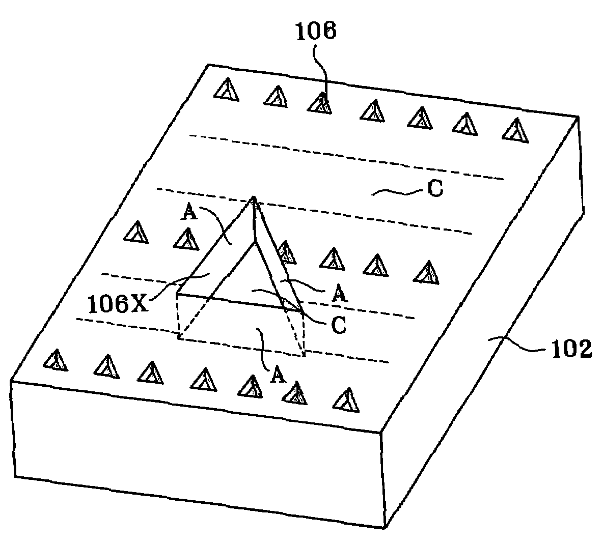
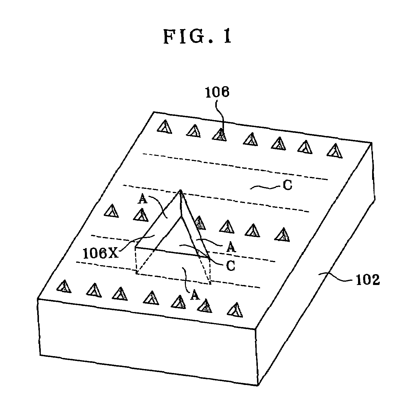
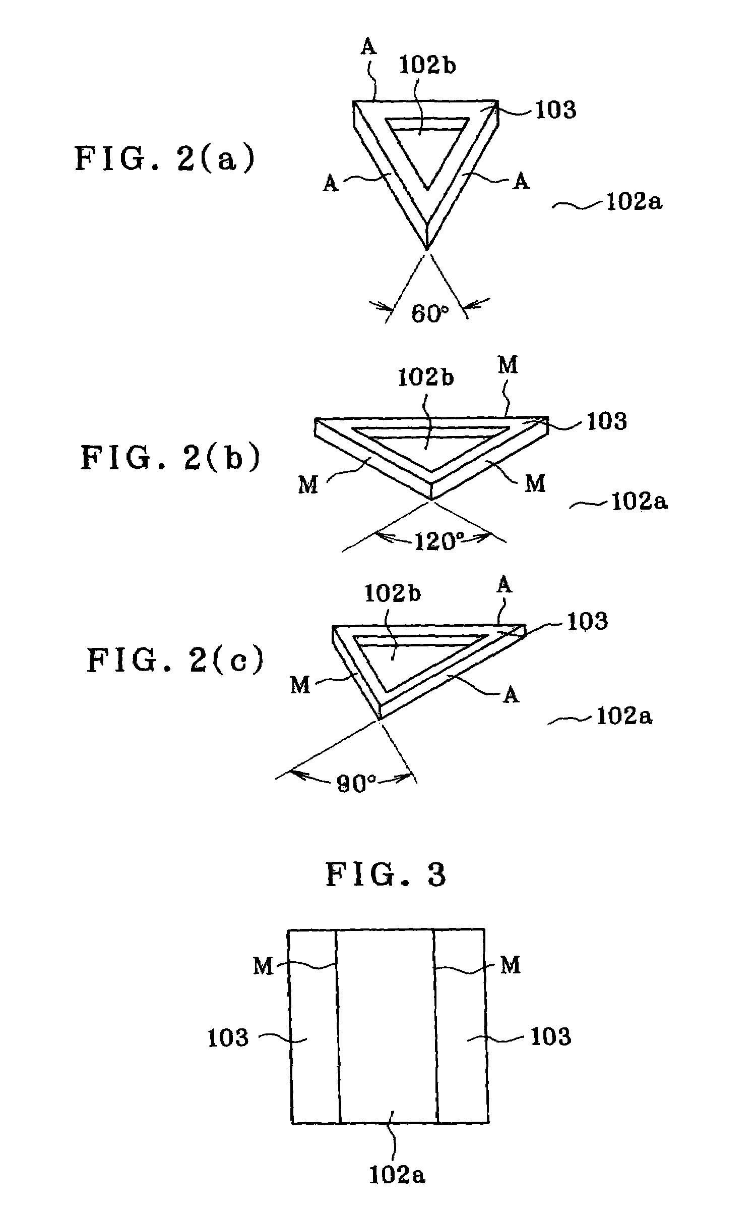
[0116]Then, a mask is used in such a way as to expose the M plane of the gallium nitride semiconductor to etch the n-type layer by RIE, thereby forming recesses. These recesses are formed in triangular, striped, and continuously corrugated forms, as shown in FIGS. 7, 8 and 9.

[0117]After formation of the recesses in the n-type gallium nitride semiconductor layer, a clad layer comprising AlGaN is formed, followed by formation of a multiple quantum well active layer formed of a combined well layer and barrier layer comprising a combination of InGaN with GaN. This active layer could have an outermost layer of eit...

example 2

B. Example 2

[0120]As in Example 1, a gallium nitride semiconductor light-emitting device comprising layers from the n-electrode to the p-electrode is obtained. A resin mixture with a YAG-containing fluorescent substance is formed on the surface of the light-emitting device, thereby obtaining a white light-emitting device having high light emission efficiency.

[0121]In this example, the wavelength conversion by the fluorescent substance is combined with the aforesaid properties of the nitride semiconductor device, so that white light can more efficiently be obtained. That is, when the active layer is formed on the C and M planes of the nitride semiconductor layer, light from the C plane has a longer wavelength. By use of a fluorescent substance such as one that absorbs the major peak wavelength of light from that C plane and excites a much longer wavelength, however, white light can be obtained through the light emitted from the M plane with a shorter wavelength and the light from the...


PUM


Abstract

The invention provides a nitride semiconductor light-emitting device comprising gallium nitride semiconductor layers formed on a heterogeneous substrate, wherein light emissions having different light emission wavelengths or different colors are given out of the same active layer. Recesses 106 are formed by etching in the first electrically conductive (n) type semiconductor layer 102 formed on a substrate with a buffer layer interposed between them. Each recess is exposed in plane orientations different from that of the major C plane. For instance, the plane orientation of the A plane is exposed. An active layer is grown and joined on the plane of this plane orientation, on the bottom of the recess and the C-plane upper surface of a non-recess portion. The second electrically conductive (p) type semiconductor layer is formed on the inner surface of the recess. With the active layer formed contiguously to the semiconductor layer in two or more plane orientations, a growth rate difference gives rise to a difference in the thickness across the quantum well (active layer), giving out light emissions having different light emission wavelength peaks or different colors.

Description

BACKGROUND OF THE INVENTION[0001]1. Field of the Invention [0002]The present invention relates generally to a nitride semiconductor device comprising a gallium nitride semiconductor layer and its fabrication process, and more particularly to a nitride semiconductor device comprising a gallium nitride semiconductor layer formed on a heterogeneous substrate, wherein light is emitted in a plurality of colors having different light emission wavelengths from an active layer.[0003]2. Related Art[0004]In recent years, nitride semiconductor devices comprising gallium nitride semiconductor layers have been put to diverse uses and available in every aspect of daily life as light-emitting diodes (LEDs) emitting light in various colors and wavelengths such as blue light, green light, white light and ultraviolet light. In particular, white LEDs have high promise for the coming generation of lighting systems superseding fluorescent lamps.[0005]In widespread nitride semiconductor devices comprisin...

Claims


Application Information

Patent Timeline
Patent Type & Authority Patents(United States)
IPC IPC(8): H01L27/15H01L33/24H01S5/02H01S5/32H01S5/343
CPCB82Y20/00H01L33/24H01S5/34333H01S5/0213H01S5/3202H01S5/3203H01S2304/12H01S5/320225
Inventor NARUKAWA, YUKIONIKI, ISAMUSCHERER, AXELOKAMOTO, KOICHIKAWAKAMI, YOICHIFUNATO, MITSURUFUJITA, SHIGEO
Owner NICHIA CORP
Why Eureka
Try Eureka