Vacuum processing method and vacuum processing apparatus

a vacuum processing and vacuum processing technology, applied in the field of vacuum processing methods and vacuum processing apparatuses, can solve problems such as displacement, deterioration of apparatus throughput, and problems in transferring wafers using such robots

Active Publication Date: 2008-04-01
HITACHI HIGH-TECH CORP
View PDF4 Cites 15 Cited by
  • Summary
  • Abstract
  • Description
  • Claims
  • Application Information

AI Technical Summary

Benefits of technology

[0012]The object of the present invention is to provide a vacuum processing apparatus or vacuum processing method having high throughput and capable of coping appropriately with the displacement of the wafer caused during hand over and transfer.
[0014]According to the present invention, the position correction quantity in the rotational direction and the position correction quantity in the advancing direction of the wafer with respect to the vacuum robot is calculated based on the outputs of the θ axis sensor and the R axis sensor, and if the quantities exceed a predetermined standard value, a position data change operation is performed to appropriately align the wafer coping with the displacement during transfer operation, and if the difference in distance data acquired based on the outputs of the θ axis sensor and the R axis sensor exceeds a permissible value, it is determined that a displacement error has occurred and the operation is stopped, according to which the invention can even cope with any unanticipated displacement of the wafer.

Problems solved by technology

On the other hand, some problems have occurred in transferring wafers using such robots.
However, according to the wafer alignment correcting system of the above-mentioned prior art, the methods utilizing sensors disposed in the R axis direction to detect the wafer position or utilizing sensors disposed in the θ axis direction to correct the wafer position had the following drawbacks.(1) Since the wafer displacement is detected by the sensors and the position of the wafer is corrected before transferring the wafer into the processing chamber, the displacement occurring after the correction of position during the transfer of the wafer cannot be corrected, and the displacement cannot be detected.(2) If the transfer speed of the wafer is slowed down before the sensor and the speed is maintained slow enough to prevent displacement of the wafer until the wafer reaches the target position, the throughput of the apparatus is deteriorated and the productivity is thereby affected.

Method used


Image

  • Vacuum processing method and vacuum processing apparatus
  • Vacuum processing method and vacuum processing apparatus
  • Vacuum processing method and vacuum processing apparatus

Examples


embodiment 1

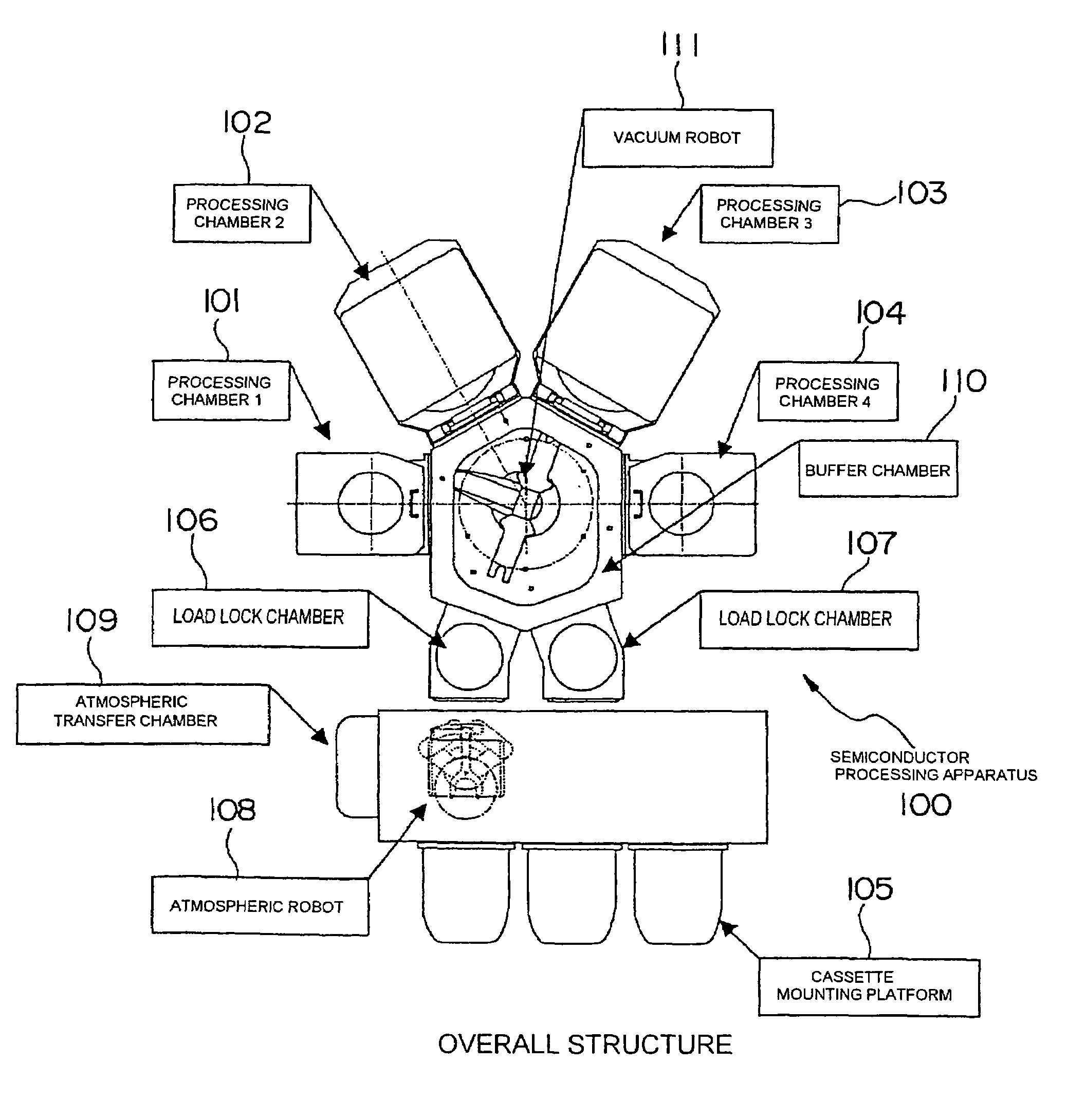
[0023]FIG. 1 is a view showing the whole structure of a semiconductor processing apparatus 100 according to embodiment 1 of the present invention.

[0024]The semiconductor processing apparatus 100 is capable of transferring wafers among a plurality of (four) processing chambers 101, 102, 103 and 104 and a plurality of (three) cassette mounting platforms 105.

[0025]The processing chambers 101, 102, 103 and 104 can be processing chambers for performing plasma etching, layer deposition and / or sputtering. The processing chambers 101, 102, 103 and 104 are each composed of a vacuum processing vessel having a sample stage for mounting a sample such as a wafer in the interior of the vessel decompressed to predetermined pressure (vacuum pressure), and by feeding processing gas into the interior of the vessel and applying an electric field or a magnetic field through an electric field or magnetic field apply means not shown, plasma is generated in the space above the wafer in the processing cham...


PUM


Abstract

The invention provides a semiconductor processing apparatus having a high throughput capable of appropriately coping with the positional displacement that may occur during transfer of the wafer after correcting the position thereof, without slowing down the transfer speed of the wafer. A position correction quantity of the wafer with respect to a vacuum robot is computed based on the outputs of a θ axis sensor for detecting the interception angle of the wafer during rotation of the vacuum robot and an R axis sensor for detecting the interception distance of the wafer during expansion and contraction of the vacuum robot. If the position correction quantity exceeds a predetermined standard value, an operation to change the position data is performed, and if the distance data obtained based on the outputs from the θ axis sensor and the R axis sensor exceeds a predetermined permissible value, it is determined that a displacement error has occurred and the operation is stopped.

Description

[0001]The present application is based on and claims priority of Japanese patent application No. 2005-313696 filed on Oct. 28, 2005, the entire contents of which are hereby incorporated by reference.BACKGROUND OF THE INVENTION[0002]1. Field of the Invention[0003]The present invention relates to an art of transferring a semiconductor processing substrate (hereinafter referred to as a wafer) among the processing chambers and the like of a semiconductor processing apparatus, and more specifically, relates to a method and apparatus for correcting the position of the wafer.[0004]2. Description of the Related Art[0005]In semiconductor device fabrication, it is preferable to connect the processing chambers or the like and have the wafer transferred among the connected processing chambers. Such transfer of the wafer is performed via a vacuum transfer apparatus for transferring the wafer from one inner chamber to another via connecting passages communicating the processing chambers and the b...

Claims


Application Information

Patent Timeline
Patent Type & Authority Patents(United States)
IPC IPC(8): G06F19/00H01L21/68
CPCH01L21/68A47J37/067A47J37/0786
Inventor NAGAYASU, NOBUOKIHARA, HIDEKIKAWAGUCHI, MICHINORIOOHIRABARU, YUUZOU
Owner HITACHI HIGH-TECH CORP
Why Eureka
Try Eureka