

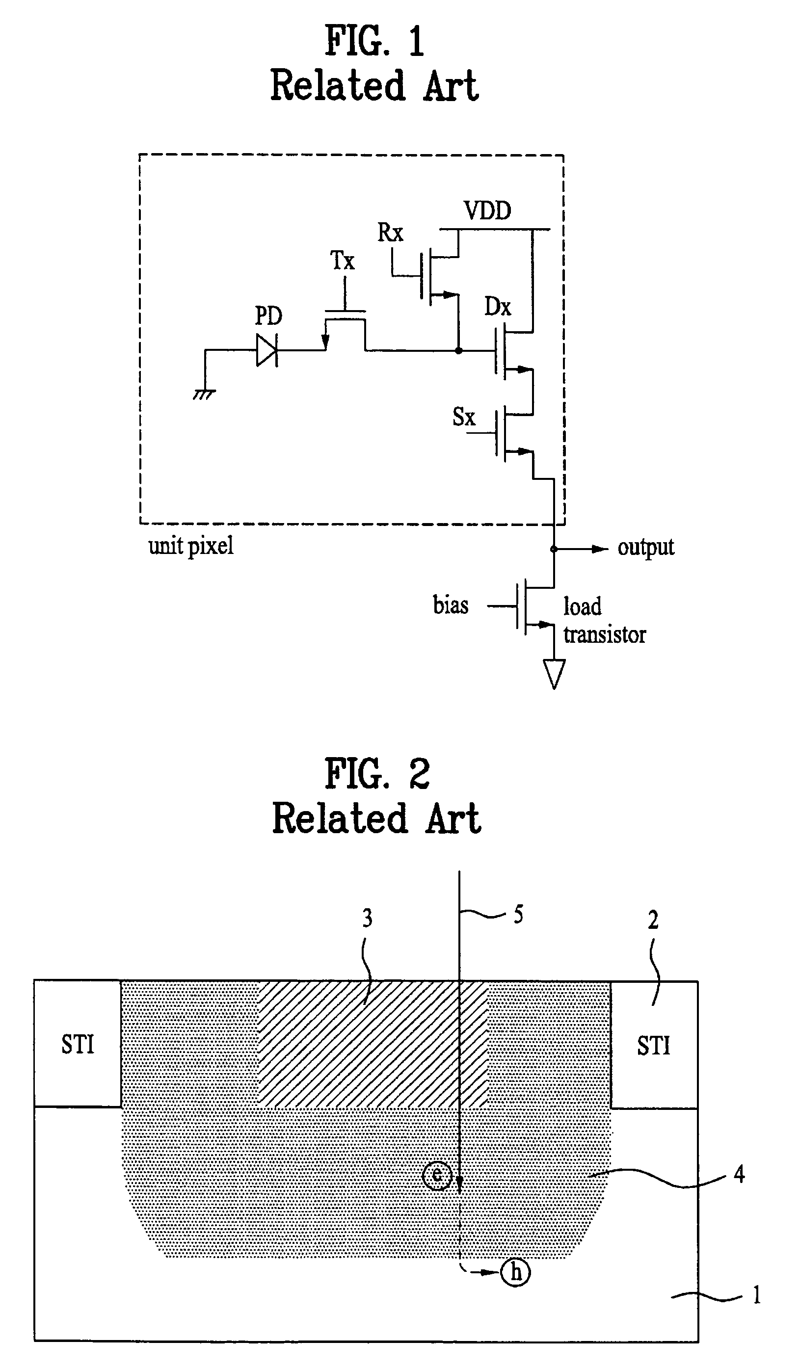
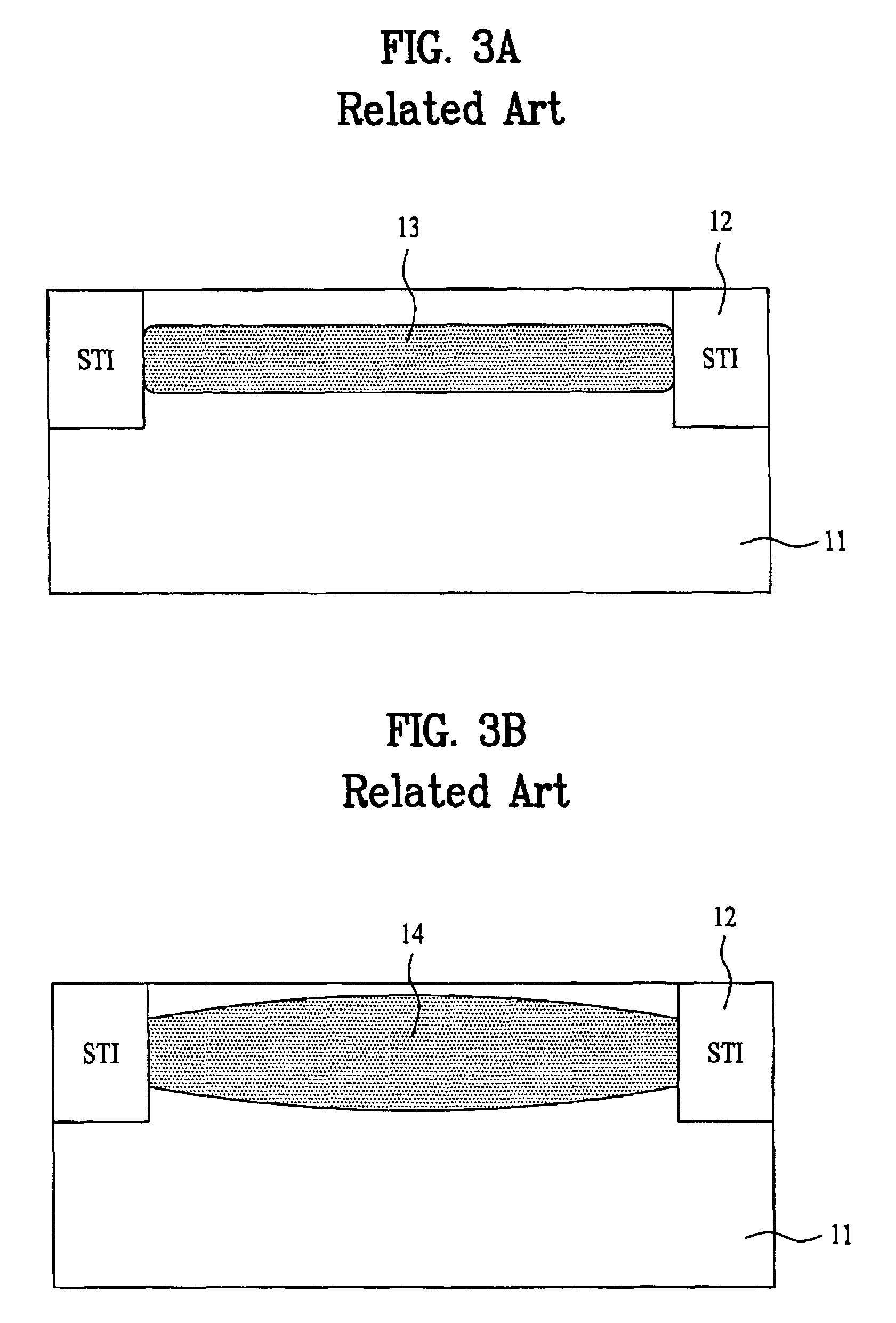
Method for fabricating photodiode of CMOS image sensor
a technology of cmos image sensor and photodiode, which is applied in the field can solve the problems of lowering high power consumption of ccd, and complicated mask process, so as to improve the sensing capacity of cmos image sensor and improve the charge accumulation capacity in the photodiode
- Summary
- Abstract
- Description
- Claims
- Application Information
AI Technical Summary
Benefits of technology
Problems solved by technology
Method used
Image

Examples
Embodiment Construction
[0036]Reference will now be made in detail to the preferred embodiments of the present invention, examples of which are illustrated in the accompanying drawings. Wherever possible, the same reference numbers will be used throughout the drawings to refer to the same or like parts.
[0037]Hereinafter, a method for fabricating a photodiode of a CMOS image sensor according to the present invention will be described with reference to the accompanying drawings.
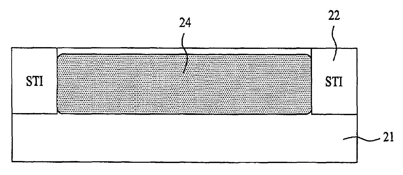
[0038]FIG. 4A to FIG. 4C are cross sectional views of the process for fabricating a photodiode of a CMOS image sensor according to the present invention.
[0039]As shown in FIG. 4A, an STI layer 22 is formed in a semiconductor substrate 21 by a trench isolation technology. As a result, the semiconductor substrate 21 is divided into an active area and a field area.
[0040]After that, impurity ions for formation of a photodiode are firstly implanted to the semiconductor substrate 21 of the active area in correspondence with the portion for ...
PUM
 Abstract
Description
Claims
Application Information