Skew free control of a multi-block SRAM

a multi-block sram and control pulse technology, applied in the field of control of multi-block semiconductor srams, can solve the problems of limiting the speed of memory operation, memory malfunction, variable skew of control pulses, etc., and achieves the effect of reducing timing skew, reducing timing skew, and speeding up memory cycle times

Inactive Publication Date: 2008-04-08
TAIWAN SEMICON MFG CO LTD
View PDF9 Cites 6 Cited by
  • Summary
  • Abstract
  • Description
  • Claims
  • Application Information

AI Technical Summary

Benefits of technology

[0011]It is the object of this invention to reduce the timing skew between memory control pulses in multi-block semiconductor memory systems.
[0012]Another object of the present invention is to use the reduced timing skews between memory control pulses to achieve faster memory cycle times.
[0013]Another object of the present invention is to use the reduced timing skews between memory control pulses to increase SRAM operational reliability.
[0014]A further object of the present invention is to use the reduced timing skews between memory control pulses to increase the SRAM chip yield.

Problems solved by technology

The differences in loading and fan-out result in variation in skew of these control pulses.
In high speed memories, these variations in loading and fan-out are significant and limit the speed of memory operation by requiring sufficient timing margins to accommodate worst case skews.
In the extreme case, the resultant skew may be large enough to cause memory malfunction.

Method used


Image

  • Skew free control of a multi-block SRAM
  • Skew free control of a multi-block SRAM
  • Skew free control of a multi-block SRAM

Examples


Embodiment Construction

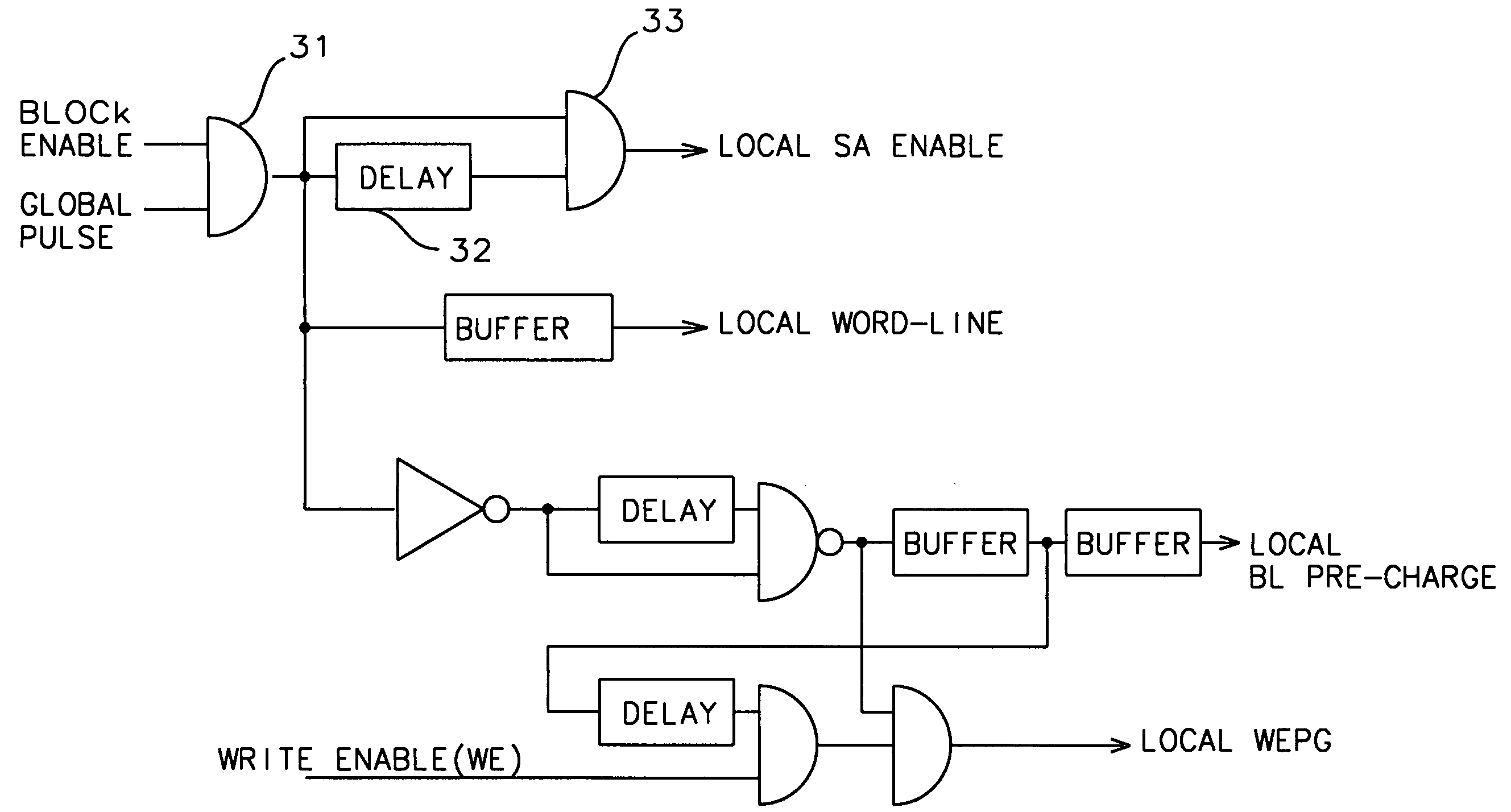
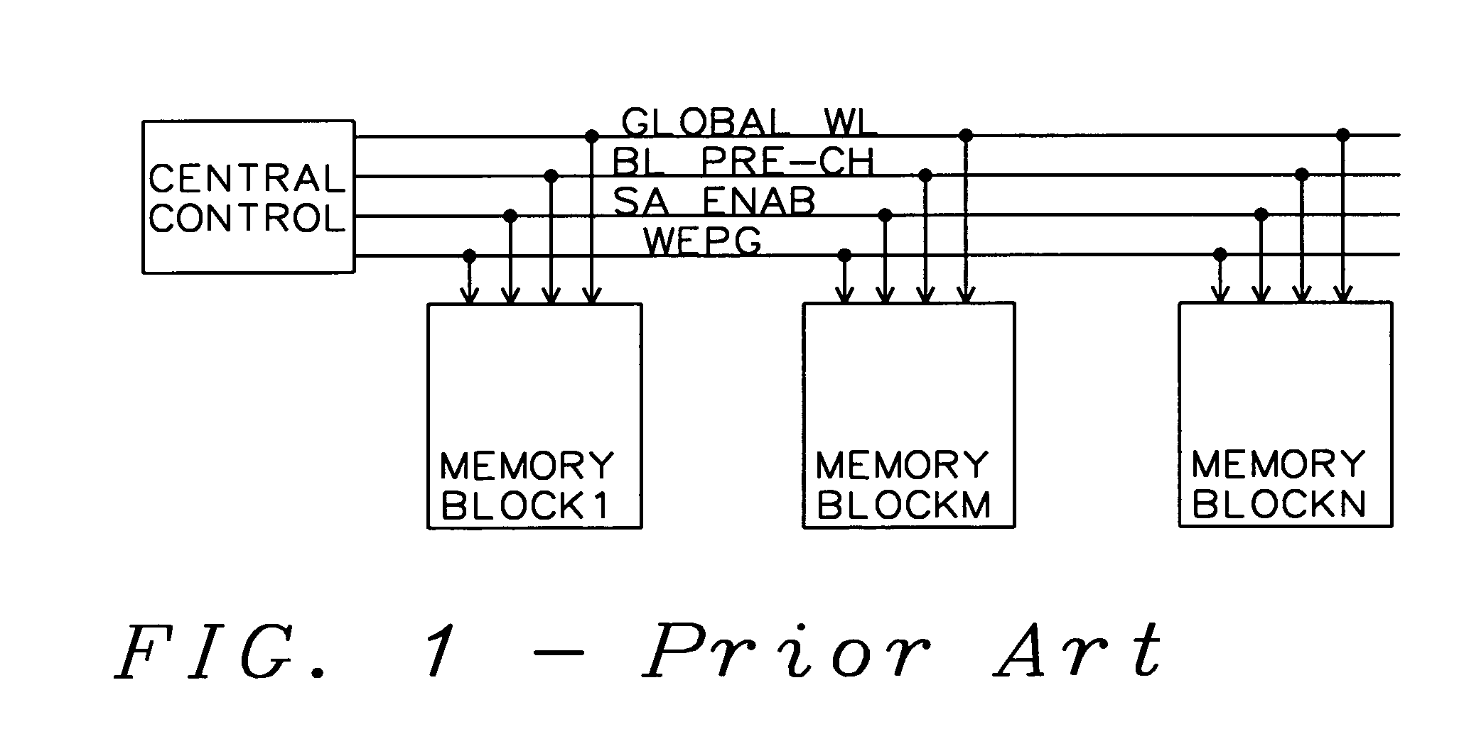
[0021]Referring now to FIG. 4, it shows a block diagram illustrating the principal components, according to the preferred embodiment of the invention, consisting of central control and a multiplicity of SRAM memory blocks. The Central Control 21 generates a single Global Pulse which is distributed to each of the memory blocks via Global Pulse Line 20. Each of the SRAM memory blocks 22, 23 and 24 in the system are identical. Each memory block contains an identical local signal generator which responds to the single global pulse and generates the required memory control pulses. Thus, SRAM memory block 23 (M) contains the local signal generator (Loc.Sig.Gen.) 25 which generates the four memory control pulses which are required for the various memory operations. These are: Word Line pulse (WL), Bit-line Pre-charge pulse (BL Prech.), Sense Amplifier Enable (SA Enab.) and Write Enable Pass Gate (WEPG).

[0022]FIG. 5 shows a block diagram of a local signal generator. A similar local signal g...


PUM


Abstract

A multi-block SRAM memory system is described where a single global clock pulse is distributed to each memory block from the central control. At each SRAM memory block a local signal generator uses the globally distributed clock pulse to generate the required memory control pulse signals. By generating the memory control pulses locally, instead of distributing these from the central control the variations in skew are greatly reduced. Thus the required timing relationship between memory control signals can be achieved with smaller timing margins. This allows higher speed memory cycle and more reliable memory operation.

Description

BACKGROUND OF THE INVENTION[0001]1. Field of the Invention[0002]This invention relates to the control of multi-block semiconductor SRAM, and more particularly to the generation of memory control pulses.[0003]2. Description of the Related Art[0004]Recent designs of Megabit semiconductor SRAM (static random access memory) are generally based on a multi-block architecture as shown in FIG. 1. The multi-block architecture design results in power saving and memory speed improvement. The central control generates global signals which are distributed to each memory block where they are used directly or are decoded to produce required local control signals. The larger the size of the SRAM, the longer the distribution paths for the global control signals. The global control pulse signals travel to each memory block and have different wire loading and fan-out loading causing a variation in delay at each memory block. Memory design requires a specific relationship between the leading and traili...

Claims


Application Information

Patent Timeline
Patent Type & Authority Patents(United States)
IPC IPC(8): G06F12/00
CPCG11C7/02G11C7/22G11C11/413
Inventor CHANG, MENG-FAN
Owner TAIWAN SEMICON MFG CO LTD
Why Eureka
Try Eureka