Substrate holding apparatus and polishing apparatus

a technology of holding apparatus and substrate, which is applied in the direction of grinding drives, grinding machine components, manufacturing tools, etc., can solve the problems of short circuit, large step height on the surface of semiconductor devices, and complicated structure of semiconductor elements, and achieve uniform polishing rate and uniform pressing force

Active Publication Date: 2008-04-15
EBARA CORP
View PDF25 Cites 50 Cited by
  • Summary
  • Abstract
  • Description
  • Claims
  • Application Information

AI Technical Summary

Benefits of technology

[0021]With the present invention having the above structure, since the stretchable and contractible portion is vertically stretched as the vertically movable member (chucking plate) is moved upwardly, the contact portion, which is held in contact with the substrate, can maintain its shape. Therefore, a contact area between the elastic member and the substrate can be kept constant, and hence it is possible to obtain a uniform pressing force over the entire surface of the substrate.
[0065]With the present invention having the above structure, the inclined portion can be easily deformed under a fluid pressure. Therefore, the inclined portion can be brought into contact with the circumferential edge of the substrate under a desired pressing force. Consequently, a polishing rate at the circumferential edge of the substrate can be controlled independently.

Problems solved by technology

In recent years, semiconductor devices have become more integrated, and structures of semiconductor elements have become more complicated.
Accordingly, irregularities on a surface of a semiconductor device become increased, so that step heights on the surface of the semiconductor device tend to be larger.
When a number of irregularities is increased on a surface of a semiconductor device, the following problems arise.
An open circuit is caused by disconnection of interconnections, or a short circuit is caused by insufficient insulation between interconnection layers.
As a result, good products cannot be obtained, and a yield tends to be reduced.
Further, even if a semiconductor device initially works normally, reliability of the semiconductor device is lowered after long-term use.
Therefore, if the irregularities of the surface of the semiconductor device are increased, then it becomes problematic in that it is difficult to form a fine pattern itself on the semiconductor device.
In such a polishing apparatus, if a relative pressing force between the semiconductor wafer being polished and the polishing surface of the polishing pad is not uniform over an entire surface of the semiconductor wafer, then the semiconductor wafer may insufficiently be polished or may excessively be polished at some portions depending on a pressing force applied to those portions of the semiconductor wafer.
Further, the polishing pad is so elastic that pressing forces applied to a peripheral portion of the semiconductor wafer being polished become non-uniform, and hence only the peripheral portion of the semiconductor wafer may excessively be polished, which is referred to as “edge rounding”.
As a hardness of the elastic membrane becomes higher, such a problem becomes worse.
Further, because of such a drawback, it is necessary to replace a worn retainer ring at an early stage, and hence a lifetime of the retainer ring is limited to a short period.
In addition to the above problem, the conventional substrate holding apparatus has another problem as follows: When a polishing process is to be started, pressurized fluid is supplied to the pressure chamber while the elastic membrane and the semiconductor wafer may not be sufficiently held in close contact with each other.
As a result, the pressurized fluid is liable to leak from a gap between the elastic membrane and the semiconductor wafer.
Further, in a process of releasing the semiconductor wafer from the top ring, the following problem arises: If a film of nitride or the like is formed on a backside surface (upper surface) of the semiconductor wafer, then the elastic membrane and the semiconductor wafer adhere to each other.
As a result, the semiconductor wafer is deformed, or broken at worst, due to a fluid pressure.
Furthermore, still another problem arises in the conventional substrate holding apparatus as follows: The pressure chamber constituted by the elastic membrane is deformed due to a fluid pressure.
Consequently, a pressing force applied to the semiconductor wafer is locally lowered, and hence a uniform polishing rate cannot be obtained over an entire polished surface of the semiconductor wafer.
As a hardness of the elastic membrane becomes higher, such a problem becomes worse.
However, because the elastic membrane having a low hardness has a low mechanical strength, the elastic membrane tends to suffer cracking, and is thus required to be replaced frequently.

Method used


Image

  • Substrate holding apparatus and polishing apparatus
  • Substrate holding apparatus and polishing apparatus
  • Substrate holding apparatus and polishing apparatus

Examples


first embodiment

[0111]A substrate holding apparatus and a polishing apparatus according to the present invention will be described in detail below with reference to the drawings.

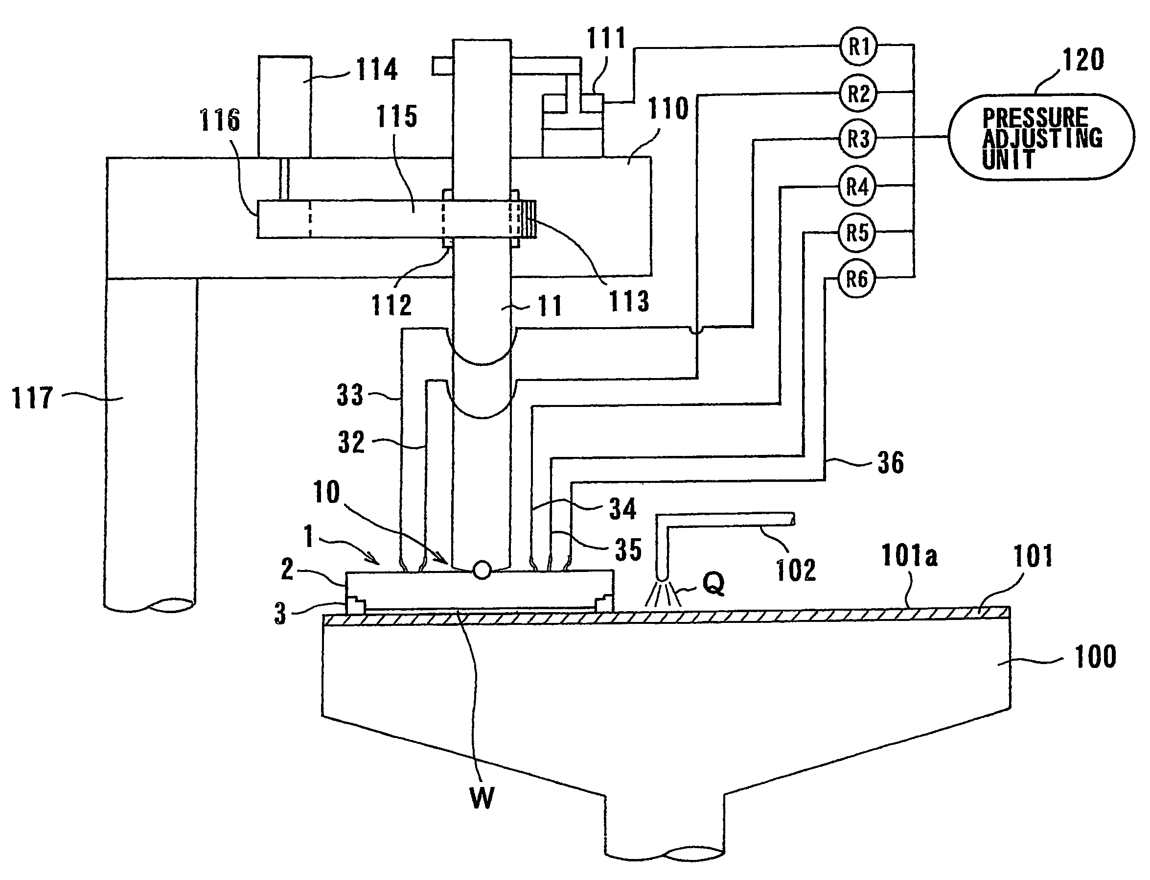
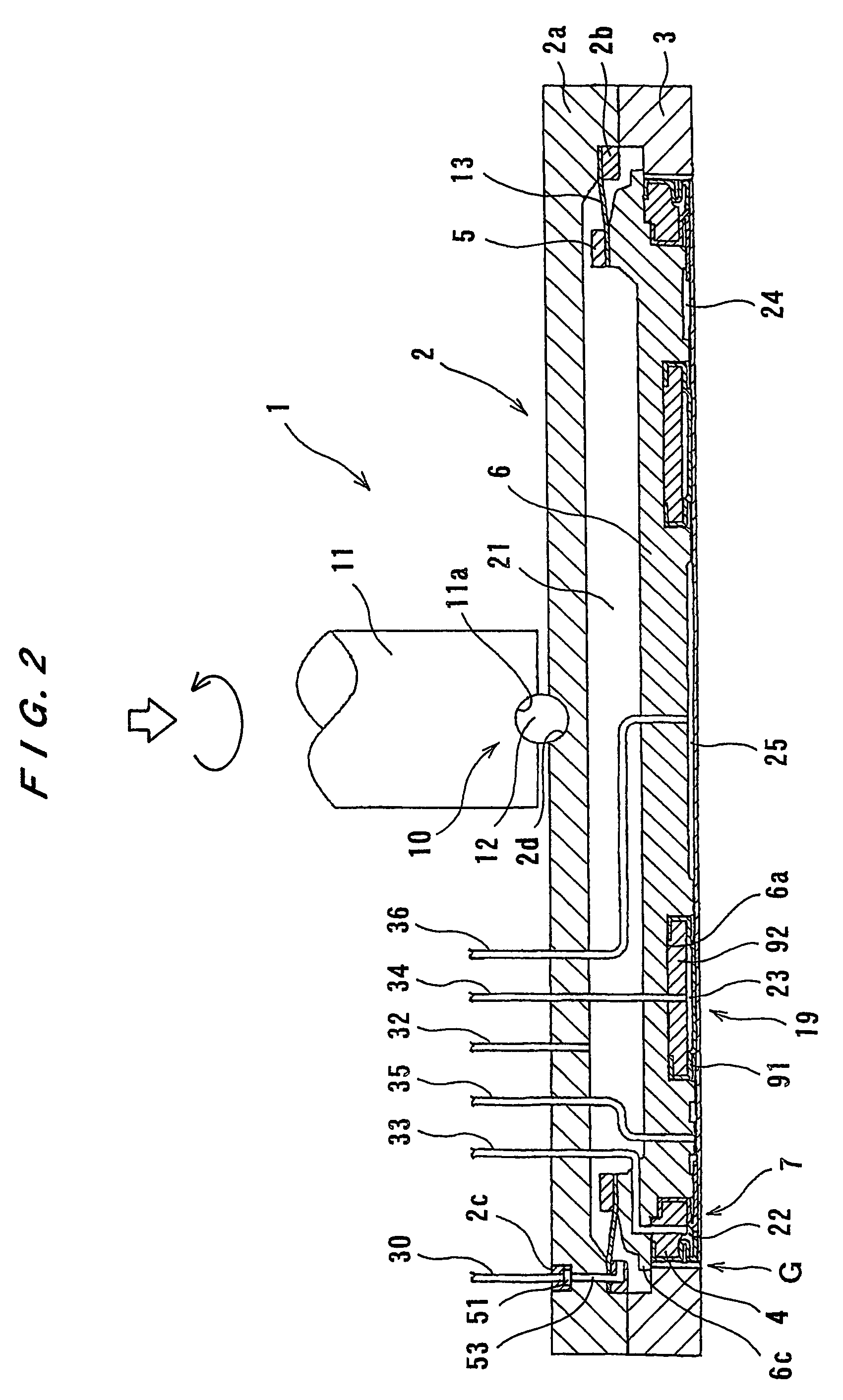
[0112]FIG. 1 is a cross-sectional view showing an entire structure of a polishing apparatus having a substrate holding apparatus according to a first embodiment of the present invention. The substrate holding apparatus serves to hold a substrate such as a semiconductor wafer to be polished and to press the substrate against a polishing surface on a polishing table. As shown in FIG. 1, a polishing table 100 having a polishing pad 101 attached on an upper surface thereof is provided underneath a top ring 1 constituting a substrate holding apparatus according to the present invention. A polishing liquid supply nozzle 102 is provided above the polishing table 100, and a polishing liquid Q is supplied onto a polishing surface 101a of the polishing pad 101 placed on the polishing table 100 from the polishing liquid supply nozzle ...

second embodiment

[0159]As shown in FIG. 6A, outer contact portion 8a constituting contact portion 8, to be pressed by pressing member 45, has a thick portion 48 on an upper surface thereof. The thick portion 48 extends in a circumferential direction of the outer contact portion 8a, and has a substantially arcuate cross section. A reinforcement member 50 for reinforcing a strength of the outer contact portion 8a is embedded in the outer contact portion 8a. The pressing member 45 has a step on a lower surface thereof to form a first pressing surface 45a and a second pressing surface 45b positioned upwardly of the first pressing surface 45a. The first pressing surface 45a is brought into contact with the outer contact portion 8a, and the second pressing surface 45b is brought into contact with the thick portion 48. The first pressing surface 45a and the second pressing surface 45b have a plurality of radially extending grooves 46a, 46b formed therein, respectively. The grooves 46a, 46b allow pressurize...

third embodiment

[0164]With this structure, while the outer contact portion 8a is being pressed by the pressing member 45, the pressurized fluid is supplied to the upper surface of the outer contact portion 8a. Therefore, as with the third embodiment described above, while edge membrane 7 is being pressed by the pressing member 45, the pressurized fluid can start pressing the outer contact portion 8a (contact portion 8).

[0165]An edge membrane according to a fifth embodiment of the present invention will be described below with reference to FIGS. 8A and 8B. FIG. 8A is a cross-sectional view showing the edge membrane according to the fifth embodiment of the present invention, and FIG. 8B is a cross-sectional view showing another structure of an edge membrane of the fifth embodiment of the present invention.

[0166]With the edge membrane according to the first embodiment, the stretchable and contractible portion is provided by folding a portion of a circumferential wall along a circumferential direction....


PUM

PropertyMeasurementUnit
diameteraaaaaaaaaa
diameteraaaaaaaaaa
diameteraaaaaaaaaa

Abstract

A substrate holding apparatus is for holding a substrate such as a semiconductor wafer in a polishing apparatus for polishing the substrate to a flat finish. The substrate holding apparatus comprises a vertically movable member, and an elastic member for defining a chamber. The elastic member comprises a contact portion which is brought into contact with the substrate, and a circumferential wall extending upwardly from the contact portion and connected to the vertically movable member. The circumferential wall has a stretchable and contractible portion which is stretchable and contractible vertically.

Description

TECHNICAL FIELD[0001]The present invention relates to a substrate holding apparatus for holding a substrate to be polished and pressing the substrate against a polishing surface, and more particularly to a substrate holding apparatus for holding a substrate such as a semiconductor wafer in a polishing apparatus for polishing the substrate to a flat finish. The present invention also relates to a polishing apparatus having such a substrate holding apparatus.BACKGROUND ART[0002]In recent years, semiconductor devices have become more integrated, and structures of semiconductor elements have become more complicated. Further, a number of layers in multilayer interconnections used for a logical system has been increased. Accordingly, irregularities on a surface of a semiconductor device become increased, so that step heights on the surface of the semiconductor device tend to be larger. This is because, in a manufacturing process of a semiconductor device, a thin film is formed on a semico...

Claims


Application Information

Patent Timeline
Patent Type & Authority Patents(United States)
IPC IPC(8): B24B7/22B24B37/30B24B37/32B24B49/16
CPCB24B37/30B24B37/32B24B49/16H01L21/304
Inventor TOGAWA, TETSUJIYOSHIDA, HIROSHINABEYA, OSAMUFUKUSHIMA, MAKOTOFUKAYA, KOICHI
Owner EBARA CORP
Why Eureka
Try Eureka