Reduced-size sensor circuit

a sensor circuit and sensor technology, applied in the field of sensors, can solve the problems of reducing the size of the overall electrical component, limiting the benefits achieved through the use of integrated circuits in terms of cost and size reduction, and using electrical circuit devices that cannot be easily implemented on integrated circuits, so as to reduce the size and/or cost of conventional sensors, reduce the number of discrete devices used, and reduce the size and/or cos

Active Publication Date: 2008-04-15
ROCKWELL AUTOMATION TECH
View PDF10 Cites 32 Cited by
  • Summary
  • Abstract
  • Description
  • Claims
  • Application Information

AI Technical Summary

Benefits of technology

[0011]The present inventor has recognized the desirability of achieving a sensor with a reduced size and / or cost, and further recognized that, in order to achieve such goals, it would be advantageous to design a sensor with fewer discrete devices and / or an integrated circuit having fewer leads / pins than are employed in conventional sensor designs. The present inventor has further recognized that many conventional sensors that utilize integrated circuits also include discrete devices that assist in preprocessing signals from a sensing device (e.g., current output by a photodiode) so that time-varying (e.g., AC) signals are provided to additional sensor processing circuitry while non-time-varying (e.g., DC) signals are filtered / rejected, and that to accommodate these discrete devices the integrated circuits often must have additional leads / pins. The present inventor has additionally recognized that such conventional sensors could be reduced in their size and / or cost, in at least some embodiments, by employing an integrated capacitor and a bias-stabilizing circuit, such that the number of discrete devices that are used could be reduced and such that the number of leads / pins of the integrated circuits could also be reduced.

Problems solved by technology

Yet the benefits achieved through the use of integrated circuits in terms of cost and size reduction often are restricted insofar as typically the integrated circuits must interface with other discrete electrical components in order to perform any desired function.
More particularly, in many applications electrical circuit devices are used that cannot be easily implemented on integrated circuits, for example, inductors, large capacitors or large resistors.
When implemented as discrete devices, these devices tend to be relatively large such that they significantly increase the size of the overall electrical component (e.g., as constructed on a circuit board).
The addition of more leads / pins can increase not only the size but also the cost of the integrated circuit.
Also, additional leads increase the susceptibility of the overall electrical component to noise.
Yet conventional sensors, and in particular conventional photosensors, typically include one or more large discrete devices such as large capacitors and large resistors that cannot be implemented on an integrated circuit.
Further, to accommodate the use of these discrete devices in conjunction with integrated circuits that are often used in such sensors, the integrated circuits typically require large numbers of leads / pins.

Method used


Image

  • Reduced-size sensor circuit
  • Reduced-size sensor circuit
  • Reduced-size sensor circuit

Examples


Embodiment Construction

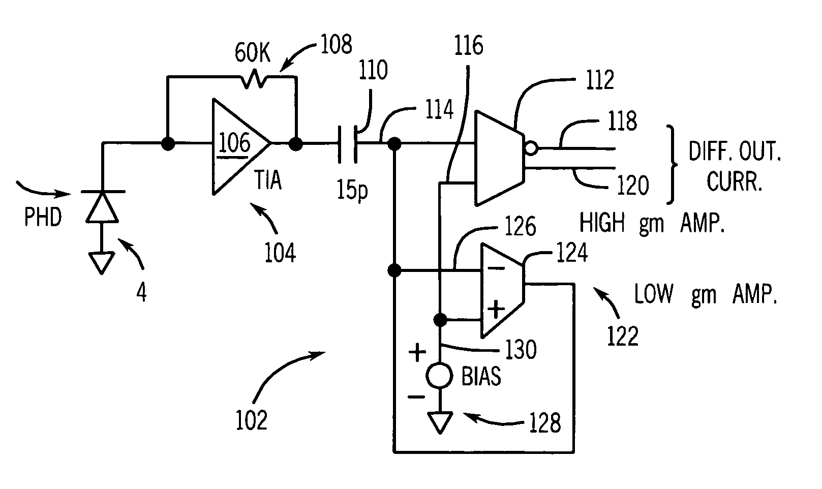
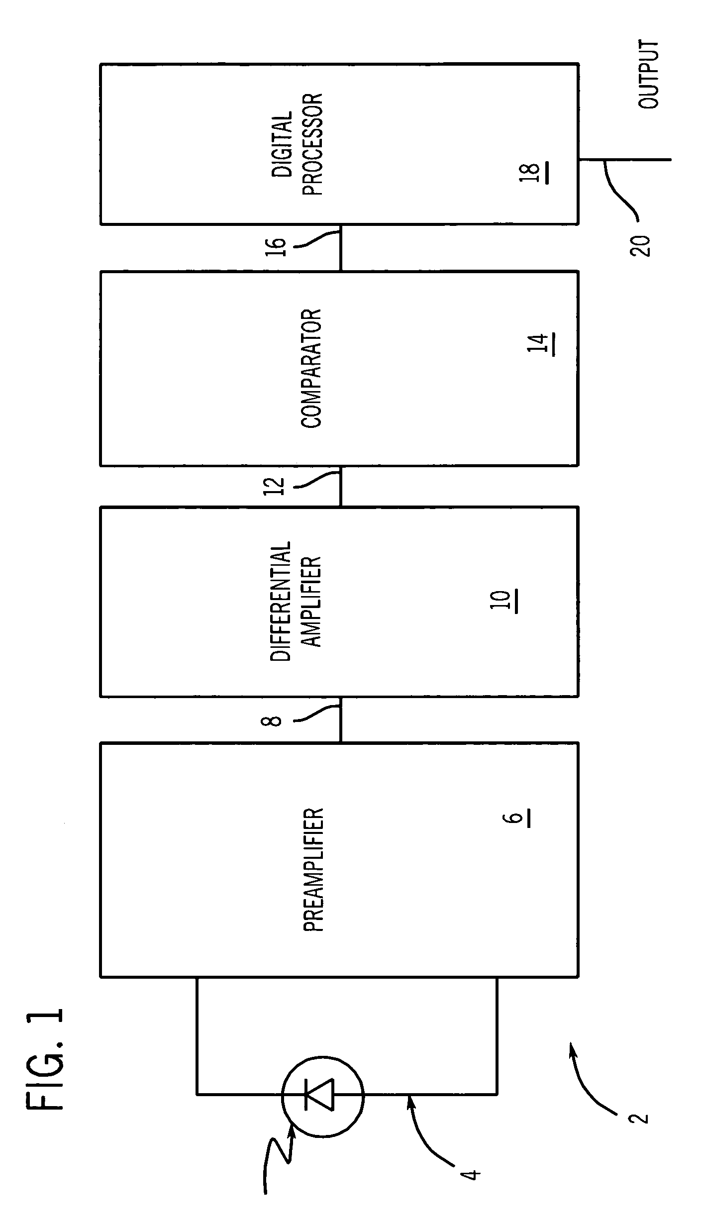
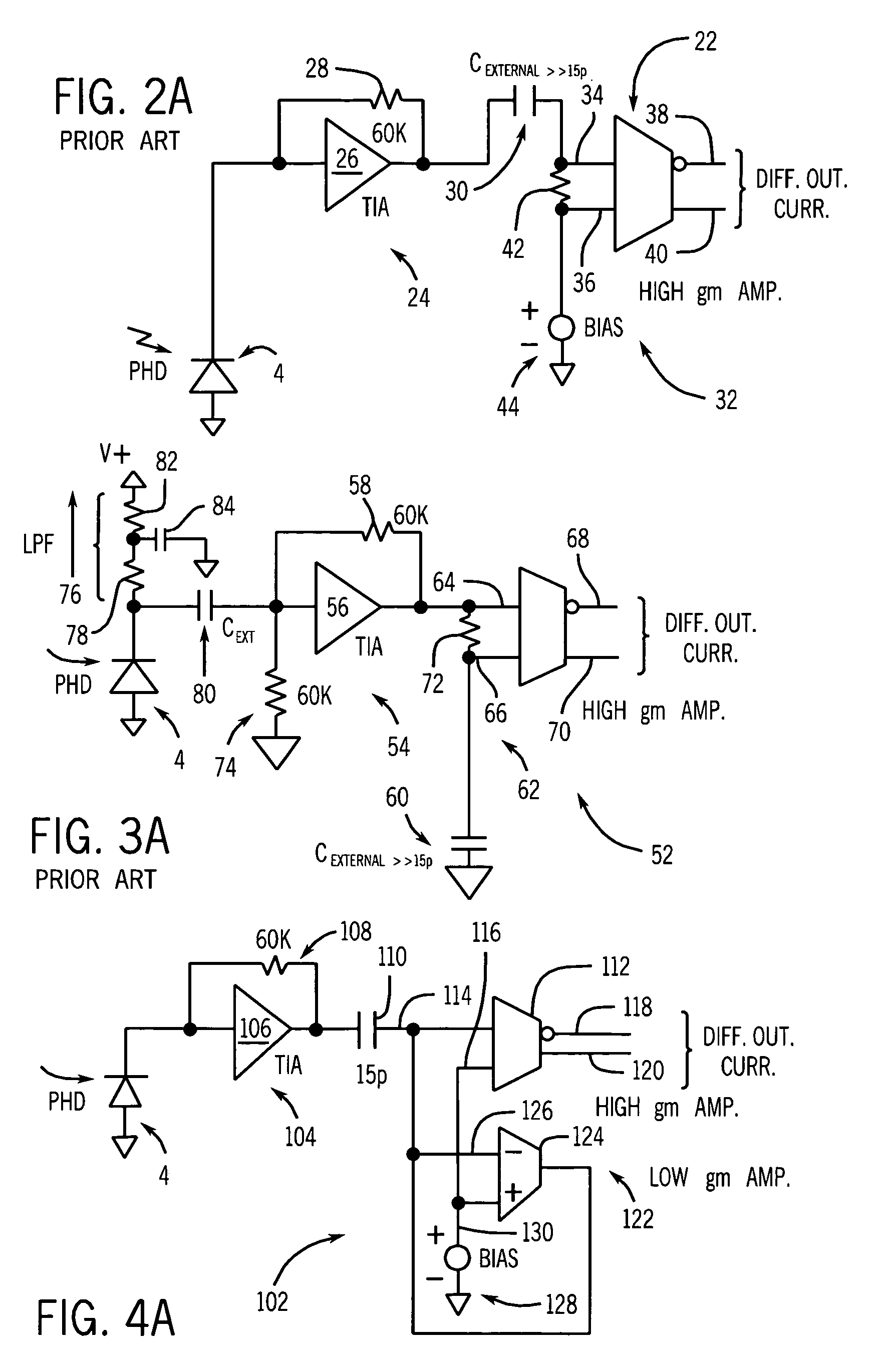
[0023]Referring to FIG. 1, a simplified block diagram of an exemplary sensor, in this case shown to be a photosensor 2, is shown. The photosensor 2 includes a sensing device 4 that in this case is a photodiode coupled to an improved preamplifier or front end amplification section 6, which in turn outputs a signal 8 (or possibly more than one signal) to a differential amplifier 10. In the present embodiment, the differential amplifier 10 outputs an additional signal (or signals) 12 to a comparator 14, which in turn outputs a further signal (or signals) 16 to a digital processor 18. The digital processor 18 then is capable of providing an output signal 20 (or potentially more than one output signal) to another device or other devices, for example, an output device such as an LCD display, a computer, the internet or some other device or system that can utilize the information output by the digital processor 18.

[0024]The preamplifier 6 serves to take a signal or signals from the photodi...


PUM


Abstract

The present invention relates to circuits configured for implementation in sensors, sensors employing such circuits, and methods of operating and manufacturing such sensors and / or circuits. In at least some embodiments, the circuit includes a capacitor having a first input terminal and a first output terminal, a first amplifier having second and third input terminals and a second output terminal, and a second amplifier having fourth and fifth input terminals and a third output terminal. The first output terminal of the capacitor is coupled at least indirectly to the second input terminal, the fourth input terminal, and the third output terminal. Additionally, the second amplifier provides feedback current with respect to the capacitor depending upon signals provided to the fourth and fifth input terminals. The capacitor and each of the amplifiers can be implemented on an integrated circuit without any need for external components.

Description

CROSS-REFERENCE TO RELATED APPLICATIONS[0001]- - -STATEMENT REGARDING FEDERALLY SPONSORED RESEARCH OR DEVELOPMENT[0002]- - -FIELD OF THE INVENTION[0003]The present invention relates to sensors and, more particularly, to sensors implemented at least in part by way of integrated circuits.BACKGROUND OF THE INVENTION[0004]Reduction of manufacturing costs and increased miniaturization continue to be important goals in the design of electrical components of a wide variety of types. Often these goals go hand-in-hand as increasing miniaturization helps to achieve reductions in the costs of assembling or implementing electrical circuitry.[0005]The use of integrated circuits in electrical components often helps to achieve both of these goals. Yet the benefits achieved through the use of integrated circuits in terms of cost and size reduction often are restricted insofar as typically the integrated circuits must interface with other discrete electrical components in order to perform any desire...

Claims


Application Information

Patent Timeline
Patent Type & Authority Patents(United States)
IPC IPC(8): H03F3/08
CPCH03F1/34H03F3/087H03F3/45179H03F3/45475H03F2200/153
Inventor ROLLINS, GEORGE E.
Owner ROCKWELL AUTOMATION TECH
Why Eureka
Try Eureka