

Display panel and method for fabricating the same
- Summary
- Abstract
- Description
- Claims
- Application Information
AI Technical Summary
Benefits of technology
Problems solved by technology
Method used
Image

Examples
embodiment 1
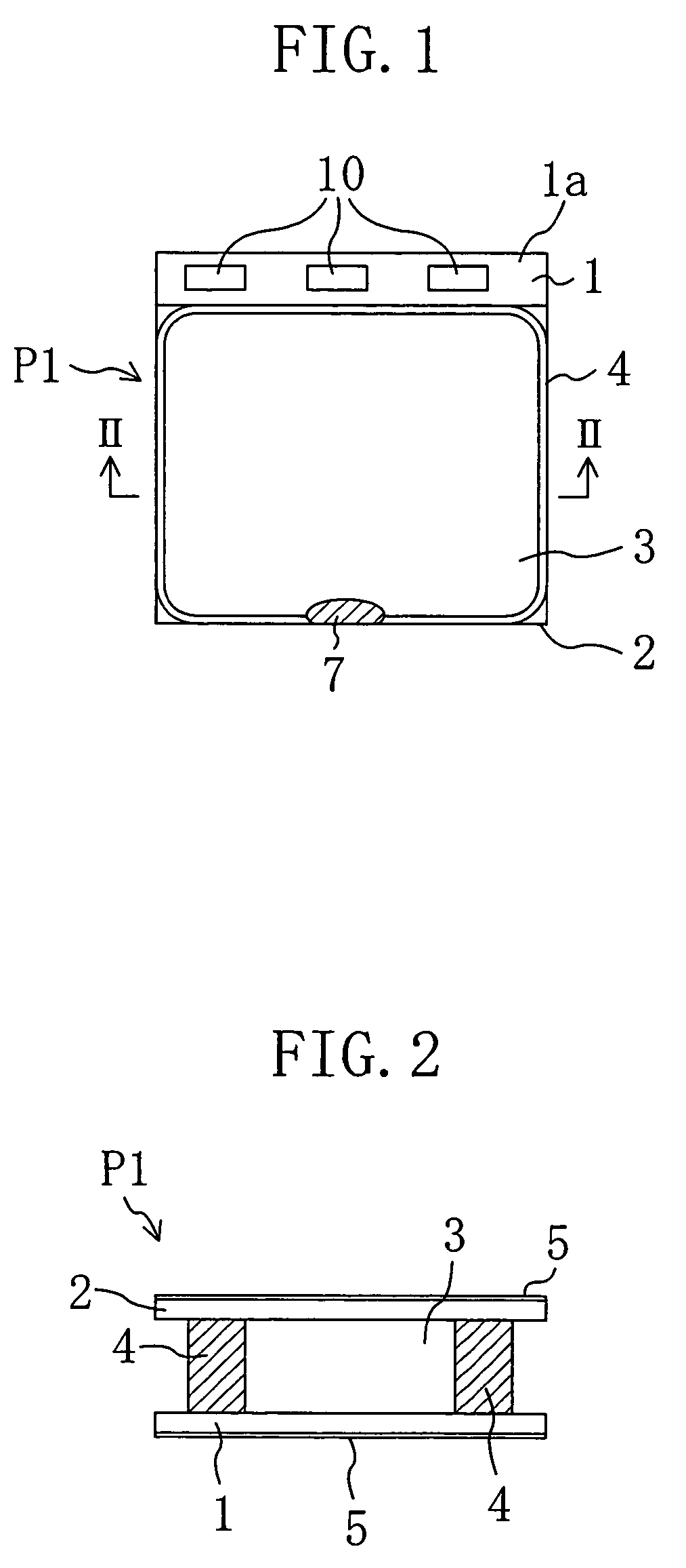
[0057]FIG. 1 is a plan view for schematically showing a liquid crystal panel P1 according to Embodiment 1, and FIG. 2 is a cross-sectional view thereof taken along line II-II of FIG. 1. This liquid crystal panel P1 includes an IC chip for driving a liquid crystal (hereinafter referred to as the “driving IC”) 10 mounted in the form of a bare chip on the liquid crystal panel P1 by the COG (Chip On Glass) method.
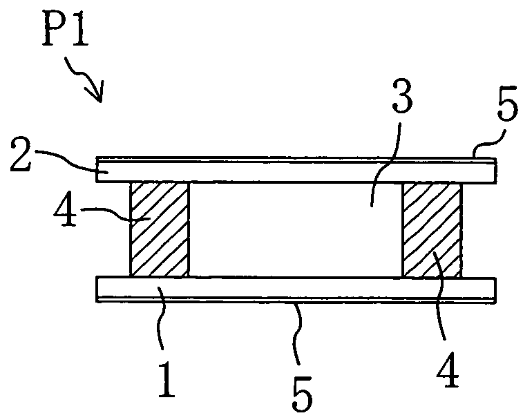
[0058]The liquid crystal panel P1 has an element substrate 1 on which a switching element is formed, a counter substrate 2 disposed to oppose the element substrate 1, and a liquid crystal layer 3 interposed between these substrates 1 and 2. The substrates 1 and 2 are aligned with a sealing material 4 sandwiched therebetween. On one face of the element substrate 1 on the side of the liquid crystal layer 3 (namely, the inner face), a plurality of pixel electrodes (not shown) arranged in the form of a matrix are formed, and on one face of the counter substrate 2 on the side of the...
embodiment 2
[0075]FIG. 5 is a cross-sectional view for schematically showing a liquid crystal panel P2 according to Embodiment 2. In the drawings referred to below, the same reference numerals are used to refer to elements with substantially like functions as those of the liquid crystal panel P1, so as to omit the description.
[0076]The liquid crystal panel P2 of this embodiment is different from the liquid crystal panel P1 of Embodiment 1 in a polarizing layer 8 formed on the inner faces of the element substrate 1 and the counter substrate 2. When the polarizing layer 8 is thus formed in the liquid crystal panel P2, polarized light can be prevented from being disturbed by in-plane variation in the substrate thickness caused by etching or variation in the thickness of the resin layer, and hence, the display quality can be prevented from being harmfully affected by disturbed polarized light. Furthermore, since the polarizing layer 8 is formed on the element substrate 1 and the counter substrate 2...
embodiment 3
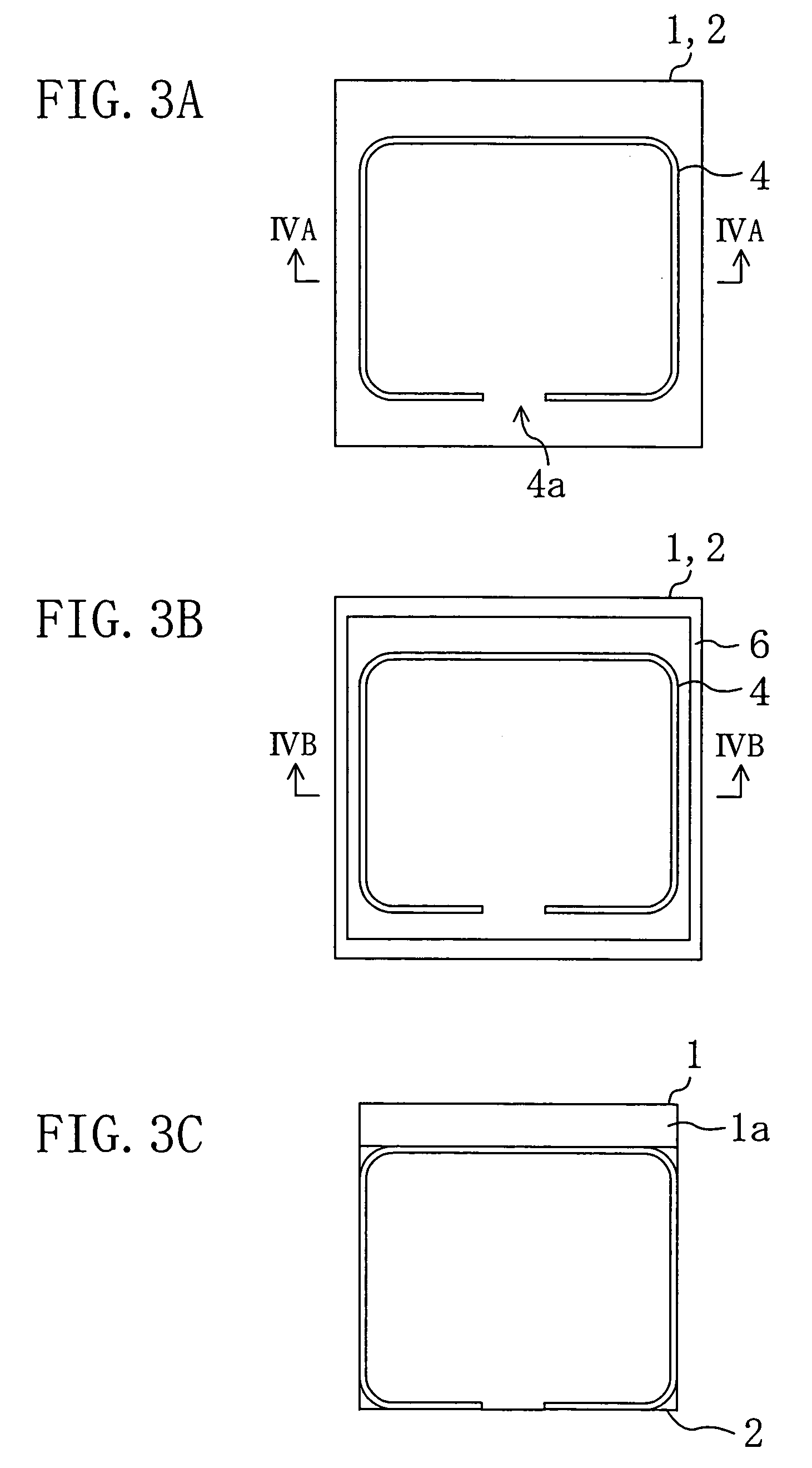
[0078]FIG. 6 is a plan view for schematically showing a liquid crystal panel P3 according to Embodiment 3, and FIG. 7 is a cross-sectional view thereof taken along line VII-VII of FIG. 6. In the liquid crystal panel P3 of this embodiment, a resin layer 5 is formed on the outer face of an element substrate 1 and the inner face of a terminal portion 1a of the element substrate 1. In other words, the resin layer 5 is formed on the both faces of the terminal portion 1a. Also, a connection part between a terminal and a driving IC 10 is covered with a resin. Since the connection part between the terminal and the driving IC 10 is reinforced by the resin coat in this manner, the connection reliability can be improved.
[0079]The fabrication process for the liquid crystal panel P3 of this embodiment will now be described with reference to the accompanying drawings. FIGS. 8A and 8B are plan views for schematically showing fabrication procedures for the liquid crystal panel P3, and FIGS. 9A, 9B ...
PUM
 Abstract
Description
Claims
Application Information