Transistors and methods of manufacture thereof

a technology of transistors and dielectric materials, applied in the field of transistors, can solve the problems of symmetric vsub>t /sub>t of a cmos device having a high k dielectric material for the gate dielectric, the device performance of the cmos device is degraded, and the success rate is small

Active Publication Date: 2008-04-22
INFINEON TECH AG +1
View PDF79 Cites 66 Cited by
  • Summary
  • Abstract
  • Description
  • Claims
  • Application Information

AI Technical Summary

Benefits of technology

[0015]Advantages of preferred embodiments of the present invention include providing novel methods of fabricating transistor devices. CMOS devices may be manufactured wherein the PMOS transistor and NMOS transistor of the CMOS devices have a substantially symmetric Vt. The gate of the NMOS transistor comprising a layer of a combination of Hf and Si sets the work function of the NMOS transistor gate electrode. The layer of the combination of Hf and Si of the gate establishes the threshold voltage Vt of the transistor.

Problems solved by technology

However, as devices are scaled down in size, using silicon dioxide for a gate dielectric becomes a problem because of gate leakage current, which can degrade device performance.
Thus, a symmetric Vt for the NMOS and PMOS transistors of a CMOS device having a high k dielectric material for the gate dielectric cannot be achieved by doping polysilicon gate material, as in SiO2 gate dielectric CMOS devices.
Fermi-pinning of high k gate dielectric material causes an assymmetric turn-on threshold voltage Vt for the transistors of a CMOS device, which is undesirable.
Efforts have been made to improve the quality of high-k dielectric films and resolve the Fermi-pinning problems, but the efforts have resulted in little success.

Method used


Image

  • Transistors and methods of manufacture thereof
  • Transistors and methods of manufacture thereof
  • Transistors and methods of manufacture thereof

Examples


Embodiment Construction

[0023]The making and using of the presently preferred embodiments are discussed in detail below. It should be appreciated, however, that the present invention provides many applicable inventive concepts that can be embodied in a wide variety of specific contexts. The specific embodiments discussed are merely illustrative of specific ways to make and use the invention, and do not limit the scope of the invention.

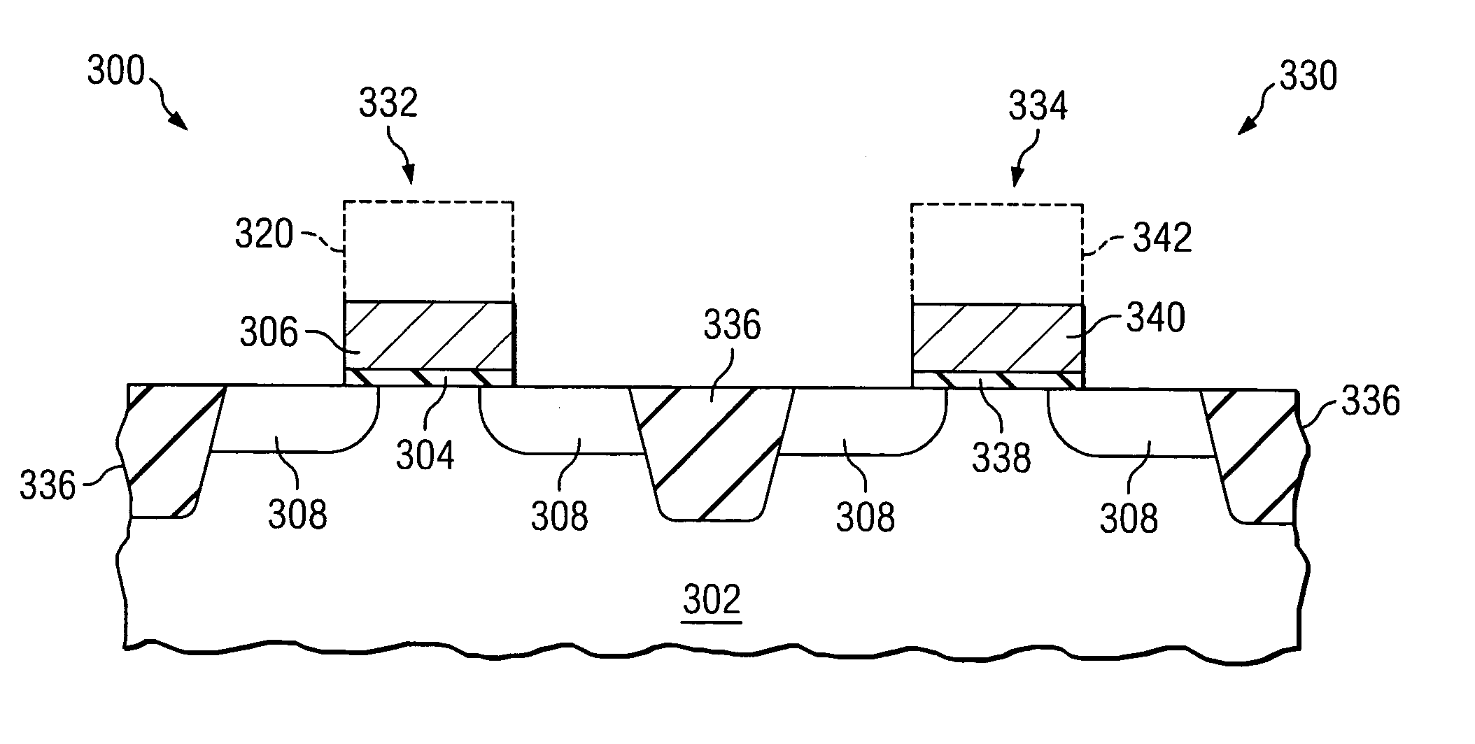
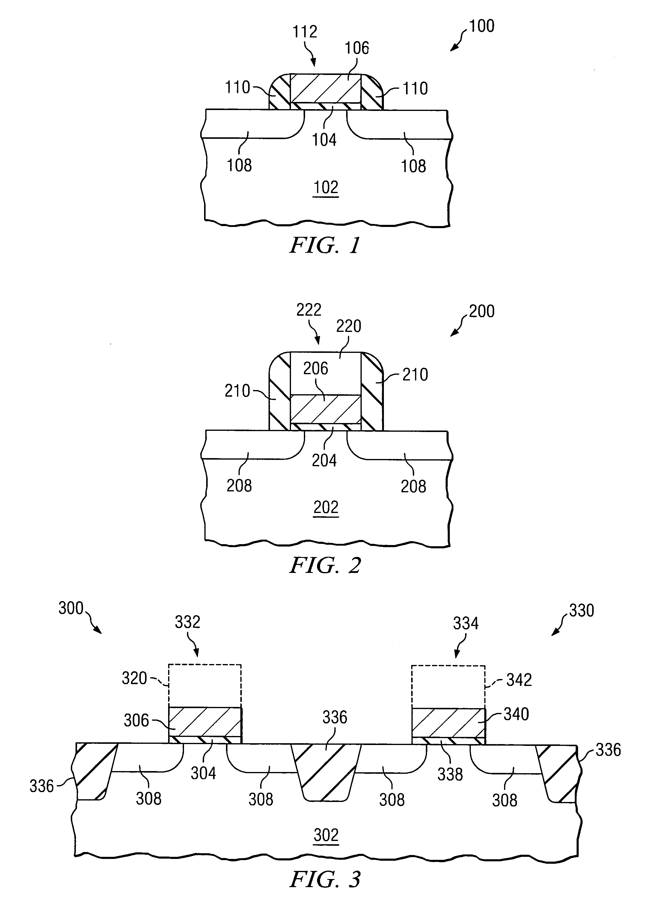
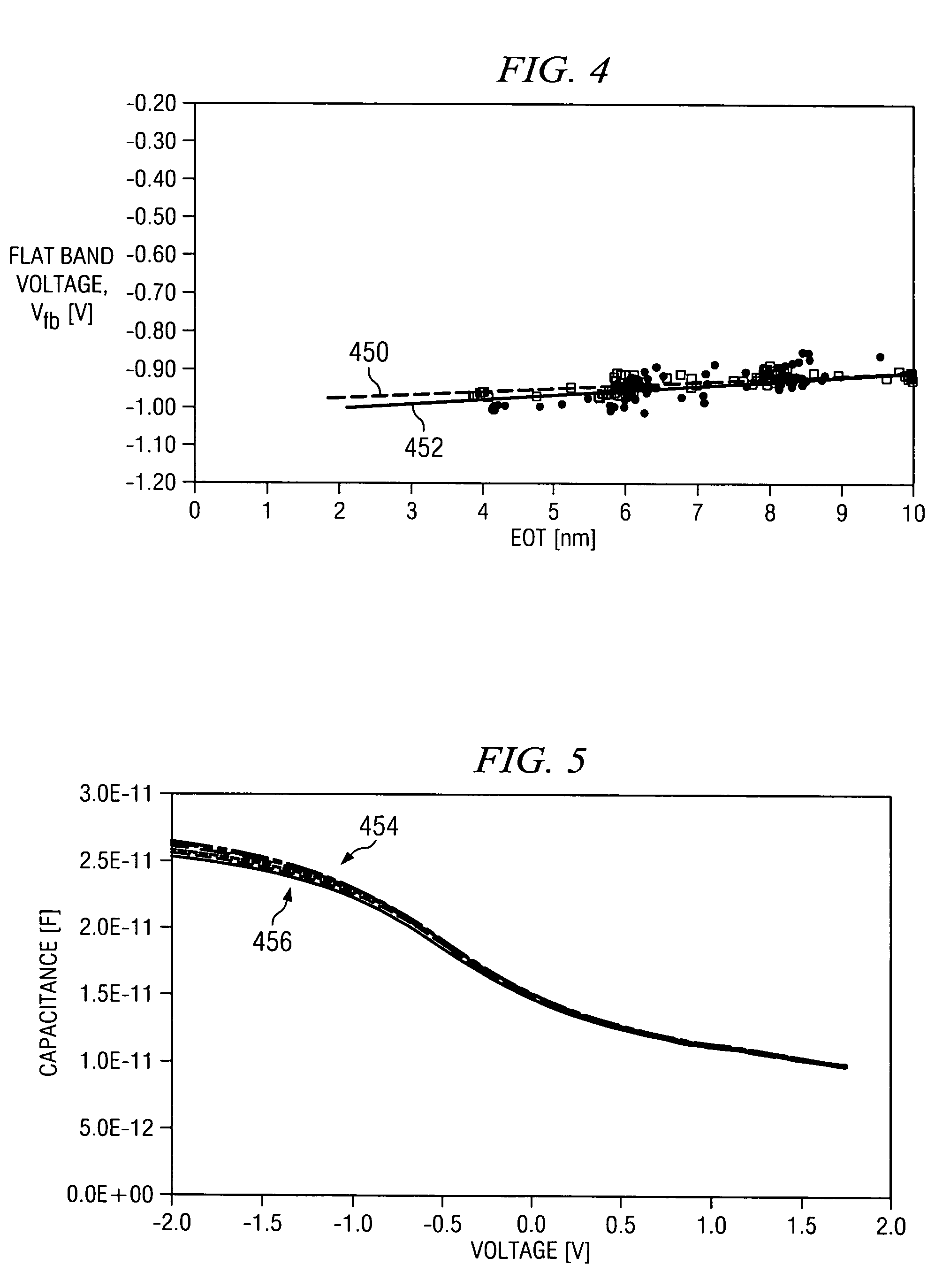
[0024]When used as a gate dielectric of a transistor, the use of high-k gate dielectric materials have generally been shown to yield orders of magnitude lower gate leakage current than SiO2 gate dielectric materials with the same effective oxide thickness (EOT). For low standby power (LSTP) and high performance (HP) applications, a high-k gate dielectric is a potential solution in the roadmap for the advanced technology nodes. High k gate dielectric materials are expected to achieve the EOT, gate leakage (Jg), mobility, and hysteresis parameters required by LSTP applications....


PUM


Abstract

Transistors and methods of manufacture thereof are disclosed. A workpiece is provided, a gate dielectric is formed over the workpiece, and a gate is formed over the gate dielectric by exposing the workpiece to a precursor of hafnium (Hf) and a precursor of silicon (Si). The gate includes and include respectively a layer of a combination of Hf and Si. The layer of the combination of Hf and Si of the gate establishes the threshold voltage Vt of the transistor. The transistor may includes and include respectively a single NMOS transistor or an NMOS transistor of a CMOS device.

Description

TECHNICAL FIELD[0001]The present invention relates generally to semiconductor devices, and more particularly to transistors and methods of manufacturing thereof.BACKGROUND[0002]Semiconductor devices are used in a variety of electronic applications, such as personal computers, cell phones, digital cameras, and other electronic equipment, as examples. Semiconductor devices are typically fabricated by sequentially depositing insulating (or dielectric) layers, conductive layers, and semiconductive layers of material over a semiconductor substrate, and patterning the various layers using lithography to form circuit components and elements thereon.[0003]A transistor is an element that is utilized extensively in semiconductor devices. There may be millions of transistors on a single integrated circuit (IC), for example. A common type of transistor used in semiconductor device fabrication is a metal oxide semiconductor field effect transistor (MOSFET).[0004]Early MOSFET processes used one t...

Claims


Application Information

Patent Timeline
Patent Type & Authority Patents(United States)
IPC IPC(8): H01L21/336H01L21/8234
CPCH01L21/28097H01L21/28194H01L21/823842H01L29/4975H01L29/517H01L29/78
Inventor LUAN, HONGFAMAJHI, PRASHANT
Owner INFINEON TECH AG
Why Eureka
Try Eureka