High electrical performance semiconductor package

a high-electricity, land-grid array technology, applied in the field of high-electricity land-grid array (lga) semiconductor packages, can solve the problems of increasing insertion loss and electromagnetic interference, affecting the electrical performance of high-frequency products, and qfn packages have encountered bottlenecks in electrical performance, so as to avoid electromagnetic noise interference, reduce the length of wires, and reduce the cost of wire bonding

Active Publication Date: 2008-04-22
SILICONWARE PRECISION IND CO LTD
View PDF10 Cites 7 Cited by
  • Summary
  • Abstract
  • Description
  • Claims
  • Application Information

AI Technical Summary

Benefits of technology

[0008]In light of the above drawbacks, an objective of the present invention is to provide a high electrical performance semiconductor package that reduces the length of bonding wires incorporated therein.
[0010]Still another objective of the present invention is to provide a high electrical performance semiconductor package that diminishes signal loss and noise interference.
[0011]A further objective of the present invention is to provide a high electrical performance semiconductor package that reduces the cost thereof.
[0015]Therefore, by the design of the fingers and the traces on the first surface of the carrier, the length of wires can be effectively reduced for a semiconductor package with double or multiple rows of lands, and the wires and traces for transmitting differential pair signals can have equal lengths and / or wire loops, such that the cost on wire bonding is decreased and insertion loss and electromagnetic noise interference are avoided as well as time for transmitting RF differential pair signals is coherent, thereby making the semiconductor package suitable for high frequency products.

Problems solved by technology

However, along with the evolution of high frequency electronic products, the QFN package has encountered bottleneck in terms of electrical performance.
This design obviously makes the wires 53″ connected to the outmost row of leads 52″ be excessively long, leading to an increase in insertion loss and electromagnetic interference.
This greatly affects the electrical performance of high frequency products, and makes the QFN package not suitable for new generation of high frequency electronic products.
This results in the same problem of electrical performance for the LGA package.
The wires 65′ connected to the outer row of lands 61′ are relatively longer and may cause insertion loss and electromagnetic interference.
Moreover, due to the different lengths of the adjacent wires 65, 65′ connected to different rows of the lands 61, 61′, time for transmitting RF differential pair signals is varied, and the signal quality would be degraded, making the LGA package not suitable for new generation of high frequency electronic products.

Method used


Image

  • High electrical performance semiconductor package
  • High electrical performance semiconductor package
  • High electrical performance semiconductor package

Examples


Embodiment Construction

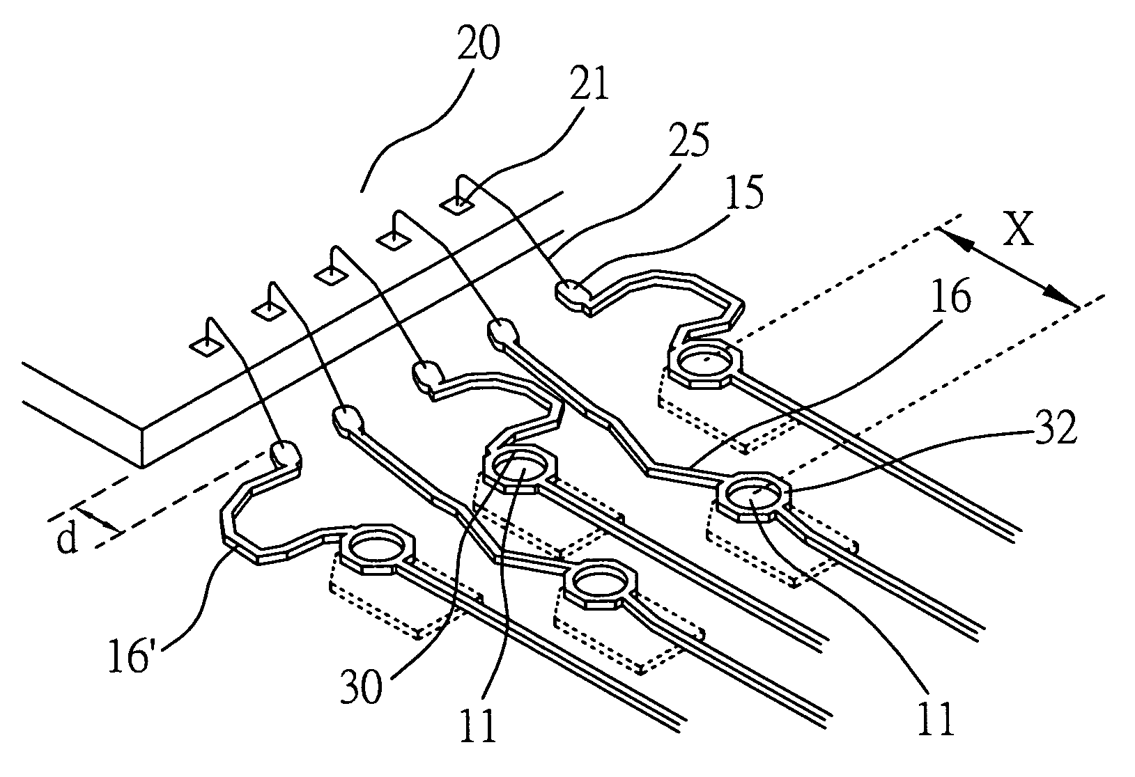
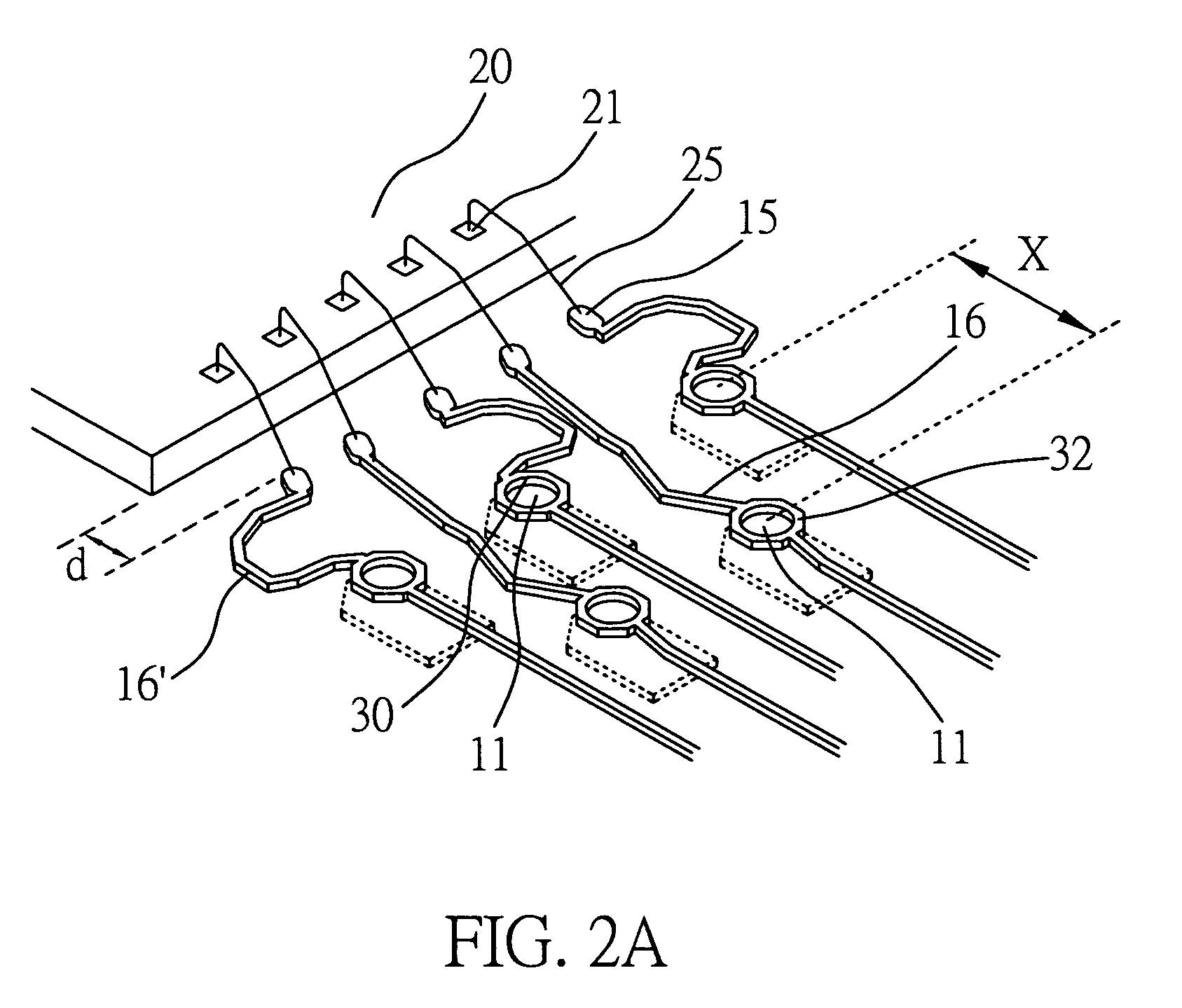
[0028]The preferred embodiment of a high electrical performance semiconductor package proposed in the preset invention is described in detail as follows with references to FIGS. 1 to 3. The signal transmission design of the high electrical performance semiconductor package is to adjust the length of adjacent bonding wires and conductive traces for transmitting differential pair signals (RF paired signals) for a high frequency chip so as to provide a uniform distance between an input terminal and an output terminal and provide different but equal-length transmission paths for the differential pair signals from the chip to the exterior of the package. As a result, the signal transmission time would not be incoherent and the signal quality can be assured no matter whether the package has double-row or multi-row electrical I / O connections.

[0029]Referring to FIG. 1, the high electrical performance semiconductor package 1 according to the present invention comprises a carrier 10, which ca...


PUM


Abstract

A high electrical performance semiconductor package is proposed. A carrier is provided having a first surface, an opposite second surface, and conductive vias for electrically connecting the first surface to the second surface. A chip is attached to the first surface of the carrier. A plurality of via lands are disposed peripherally on the first surface of the carrier and electrically connected to the vias. A plurality of conductive regions are disposed on the second surface of the carrier and electrically connected to the vias. A plurality of fingers are disposed around the chip and electrically connected to the via lands by conductive traces formed on the first surface of the carrier. A plurality of bonding wires electrically connect the chip to the fingers. Lengths of the wires for transmitting differential pair signals are substantially equal, and lengths of the traces for transmitting the differential pair signals are substantially equal.

Description

FIELD OF THE INVENTION[0001]The present invention relates to high electrical performance semiconductor packages, and more particularly, to a high electrical performance land grid array (LGA) semiconductor package for high frequency products.BACKGROUND OF THE INVENTION[0002]In the semiconductor packaging field, improvement in electrical transmission is always considered as an important factor for advancing the performance of electronic products. For example of the QFN (Quad Flat Non-leaded) technology disclosed in U.S. Pat. Nos. 5,942,794, 6,081,029 and 6,281,047, which improves a conventional lead-frame-based package such as QFP (Quad Flat Package) to allow a bottom surface of the lead frame to be directly exposed and reduce the length of leads of the lead frame, such that signal paths can be shortened and noises are diminished as well as a chip incorporated in the package can be made similar in size to a carrier, thereby facilitating the development of Chip Scale Package (CSP).[000...

Claims


Application Information

Patent Timeline
Patent Type & Authority Patents(United States)
IPC IPC(8): H05K1/16H01L23/10H01L23/367H01L23/498
CPCH01L24/49H01L23/49838H01L23/3677H01L23/49816H01L2224/48247H01L2224/48227H01L2924/014H01L2924/01033H01L24/48H01L2924/01082H01L2224/49433H01L2224/49171H01L2224/48091H01L23/49827H01L2924/00014H01L2924/00H01L2224/05554H01L2924/181H01L2224/45099H01L2224/05599H01L2924/00012
Inventor CHIANG, WEN-JUNGCHEN, CHIEN-TEWANG, YU-PO
Owner SILICONWARE PRECISION IND CO LTD
Why Eureka
Try Eureka