Luminescent ceramic for a light emitting device

a technology of light-emitting devices and luminescent ceramics, which is applied in the direction of solid-state devices, discharge tubes/lamp details, x-ray tubes, etc., can solve the problems of reducing the light extraction efficiency of the device, undesired alteration of the appearance of the light emitted from the device, and using organic encapsulants, etc., to achieve less scattering, less sensitive to temperature, and increase conversion efficiency

Active Publication Date: 2008-04-22
LUMILEDS
View PDF14 Cites 342 Cited by
  • Summary
  • Abstract
  • Description
  • Claims
  • Application Information

AI Technical Summary

Benefits of technology

[0009]In accordance with embodiments of the invention, a semiconductor light emitting device comprising a light emitting layer disposed between an n-type region and a p-type region is combined with a ceramic layer which is disposed in a path of light emitted by the light emitting layer. The ceramic layer is composed of or includes a wavelength converting material such as a phosphor. Luminescent ceramic layers according to embodiments of the invention may be more robust and less sensitive to temperature than prior art phosphor layers. In addition, luminescent ceramics may exhibit less scattering and may therefore increase the conversion efficiency over prior art phosphor layers.

Problems solved by technology

As III-nitride LEDs are operated at higher power and higher temperature, the transparency of the organic encapsulants used in layer 20 tend to degrade, undesirably reducing the light extraction efficiency of the device and potentially undesirably altering the appearance of the light emitted from the device.
However, one major disadvantage of prior solutions is the optical heterogeneity of the phosphor / encapsulant system, which leads to scattering, potentially causing losses in conversion efficiency.

Method used


Image

  • Luminescent ceramic for a light emitting device
  • Luminescent ceramic for a light emitting device
  • Luminescent ceramic for a light emitting device

Examples


example

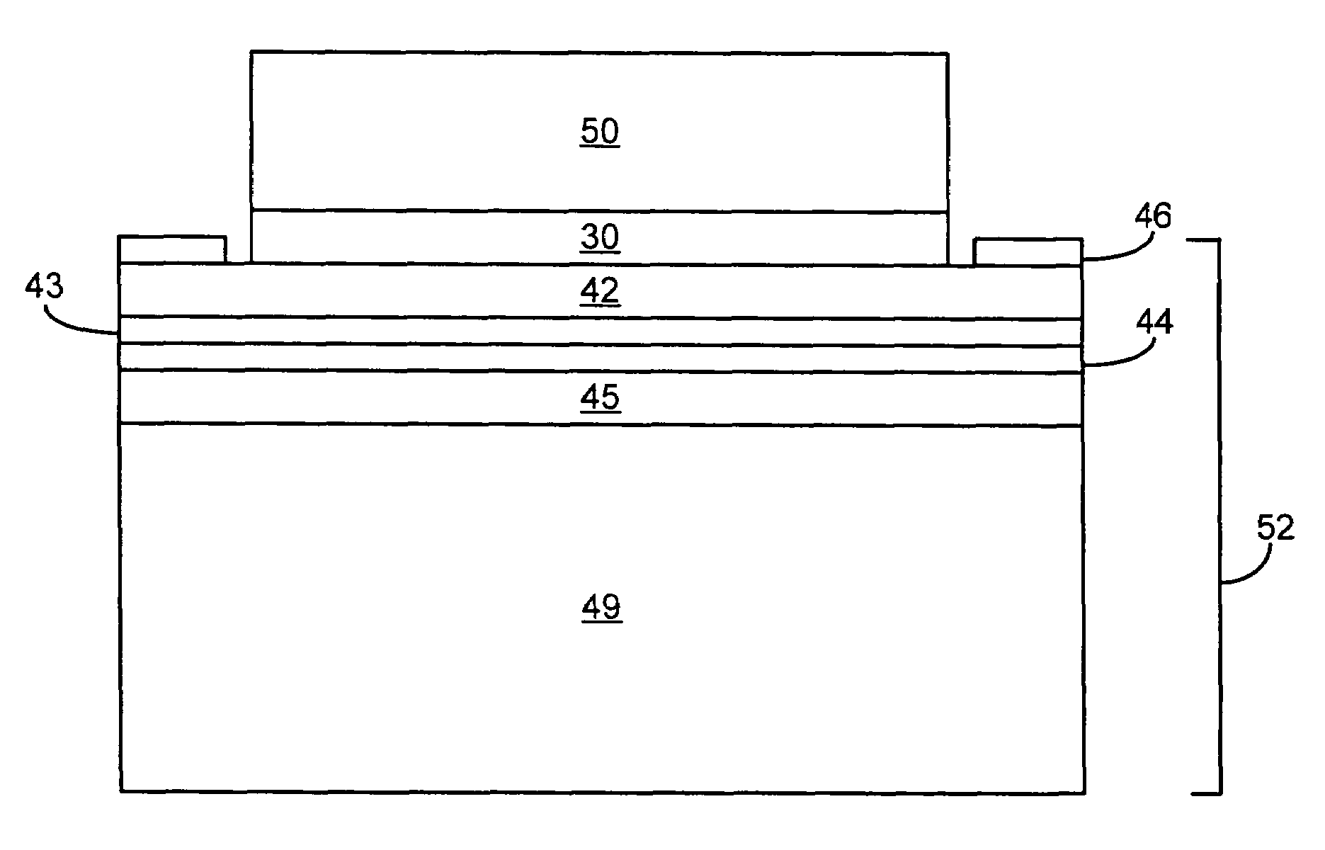
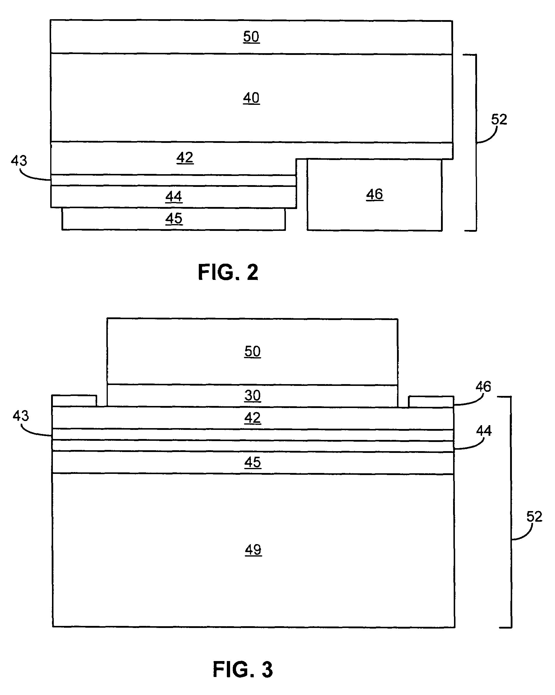
[0035]An example of a cerium-doped yttrium aluminum garnet ceramic slab diffusion-bonded to a sapphire substrate is given below.

[0036]Diffusion-bonded YAG-sapphire composites are advantageous because of their high mechanical strength and excellent optical quality. According to the phase diagram yttria-alumina within the composition range Al2O3 and 3Y2O35Al2O3, no other phase exists except an eutecticum with 33% Al. Therefore, a sinterbonded YAG-sapphire composite has an average refractive index at the (eutectoidic) interface between YAG ceramic (ni=1.84) and sapphire substrate (ni=1.76) and thus a high quality optical contact can be obtained. In addition, because of the similar expansion coefficients of YAG and sapphire (YAG: 6.9×10⁻⁶ K−1, Al2O3:8.6×10⁻⁶ K−1), sinterbonded wafers with low mechanical stress can be produced.

[0037]A diffusion-bonded YAG:Ce ceramic-sapphire wafer may be formed as follows:

[0038]a) Production of YAG:Ce ceramic: 40 g Y2O3 (99.998%), 32 g Al2O3 (99.999%), a...


PUM

PropertyMeasurementUnit
temperaturesaaaaaaaaaa
refractive indicesaaaaaaaaaa
diameteraaaaaaaaaa

Abstract

A semiconductor light emitting device comprising a light emitting layer disposed between an n-type region and a p-type region is combined with a ceramic layer which is disposed in a path of light emitted by the light emitting layer. The ceramic layer is composed of or includes a wavelength converting material such as a phosphor. Luminescent ceramic layers according to embodiments of the invention may be more robust and less sensitive to temperature than prior art phosphor layers. In addition, luminescent ceramics may exhibit less scattering and may therefore increase the conversion efficiency over prior art phosphor layers.

Description

BACKGROUND[0001]1. Field of Invention[0002]The present invention relates to wavelength converted semiconductor light emitting devices.[0003]2. Description of Related Art[0004]Light emitting diodes (LEDs) are well-known solid state devices that can generate light having a peak wavelength in a specific region of the light spectrum. LEDs are typically used as illuminators, indicators and displays. Traditionally, the most efficient LEDs emit light having a peak wavelength in the red region of the light spectrum, i.e., red light. However, III-nitride LEDs have been developed that can efficiently emit light having a peak wavelength in the UV to green region of the spectrum. III-nitride LEDs can provide significantly brighter output light than traditional LEDs.[0005]In addition, since light from III-nitride devices generally has a shorter wavelength than red light, the light generated by the III-nitride LEDs can be readily converted to produce light having a longer wavelength. It is well k...

Claims


Application Information

Patent Timeline
Patent Type & Authority Patents(United States)
IPC IPC(8): H01L27/15H01L29/22C04B35/44C04B35/547C04B35/584C04B35/597C04B35/645H01L33/50H01L33/58H01L33/64
CPCC04B35/44H01L33/505C04B35/584C04B35/597C04B35/6268C04B35/64C04B35/645C09K11/7774H01L33/501C04B35/547C04B2235/3213C04B2235/3224C04B2235/3225C04B2235/3286C04B2235/6027C04B2235/662H01L33/58H01L33/644H01L2924/0002H01L2924/00H01L33/0075H01L33/50H01L33/0093C04B2235/3217C04B2235/3229H01L33/007H01L33/06H01L33/12H01L33/32H01L33/502H01L33/508H01L33/54H01L33/56H01L33/62H01L33/641H01L2933/0041H01L2933/005H01L2933/0066H01L2933/0075
Inventor MUELLER, GERD O.MUELLER-MACH, REGINA B.KRAMES, MICHAEL R.SCHMIDT, PETER J.BECHTEL, HANS-HELMUTMEYER, JOERGDE GRAAF, JANKOP, THEO ARNOLD
Owner LUMILEDS
Why Eureka
Try Eureka