Optical scanning device with at least one resin lens for controlling a beam waist position shift

a scanning device and a technology of resin lenses, applied in the direction of condensers, instruments, mountings, etc., can solve the problems of resin lenses being susceptible to environmental conditions, changing shape, and degrading image quality,

Active Publication Date: 2008-04-22
RICOH KK
View PDF37 Cites 29 Cited by
  • Summary
  • Abstract
  • Description
  • Claims
  • Application Information

AI Technical Summary

Problems solved by technology

This tendency of the lens characteristics to vary with temperature fluctuations or wavelength variation results in a large beam spot and causes the image focus location (point of focus) of the beam spot to vary, degrading the quality of the image.
However, on the flipside, resin lenses are susceptible to variations in environmental conditions, and particularly, change shape and have varying refractive indices with change in the temperature.
Consequently, their optical characteristics, and particularly, the power, deviate from the design value, thus causing a variation in the “beam spot diameter” which is the laser spot diameter on the surface being scanned.
The variation in the wavelength gives rise to chroma aberration of the optical system used in the optical scanning device, which in turn results in a variation in the beam spot diameter.
Therefore, when employing a collimator lens as a power diffractive surface, such as in the instance disclosed as a comparative example in Patent document 2, or in Japanese Patent Laid-Open Publication No. 2000-171741, there is a risk of an adverse effect in the form of “degradation of wavefront aberration of the collimated light beam”.
Since degradation of wavefront aberration includes the effect of increasing the beam spot diameter, using collimating lens poses a problem for high resolution images for which a very small beam spot diameter is a prerequisite.
Consequently, the effect of variation in the emission wavelength of the semiconductor laser device on imaging in the main scanning direction and the sub-scanning direction cannot be adjusted independently.
The process of forming a diffractive surface on an operative area of the long lens is a time-consuming one as a large area needs to be covered, the low production rate of the lens pushing up the cost.

Method used


Image

  • Optical scanning device with at least one resin lens for controlling a beam waist position shift
  • Optical scanning device with at least one resin lens for controlling a beam waist position shift
  • Optical scanning device with at least one resin lens for controlling a beam waist position shift

Examples


first working example

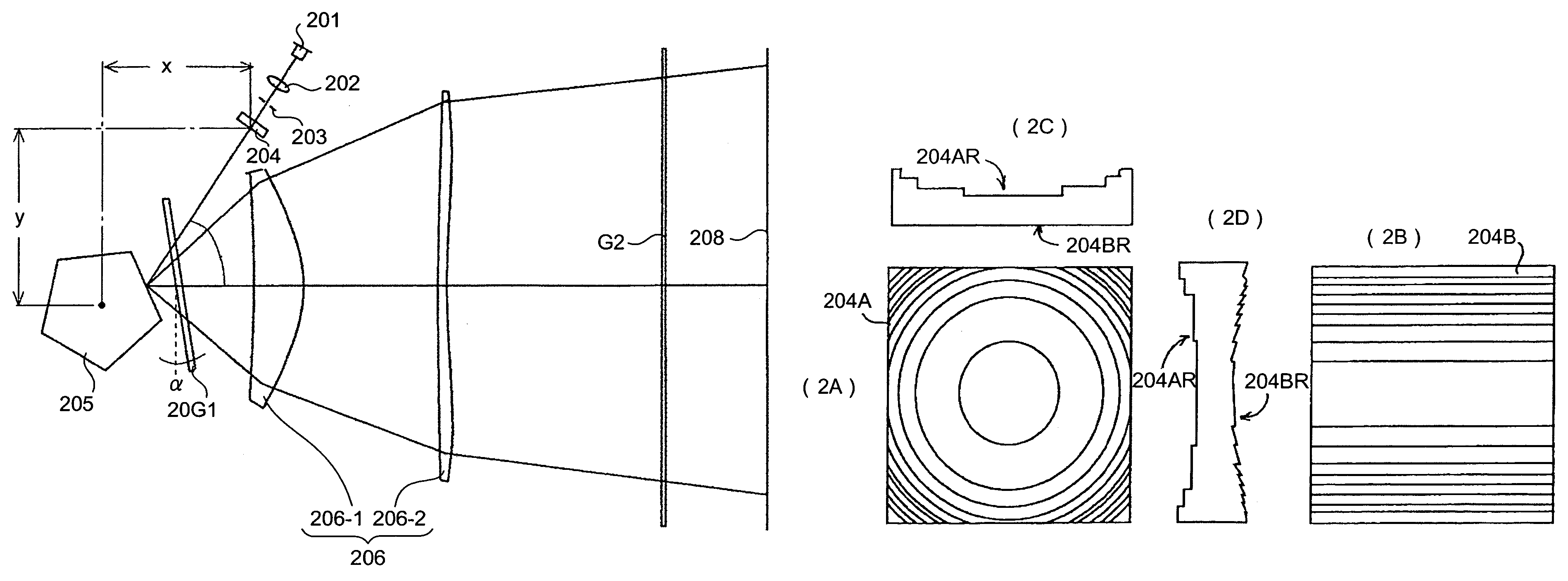
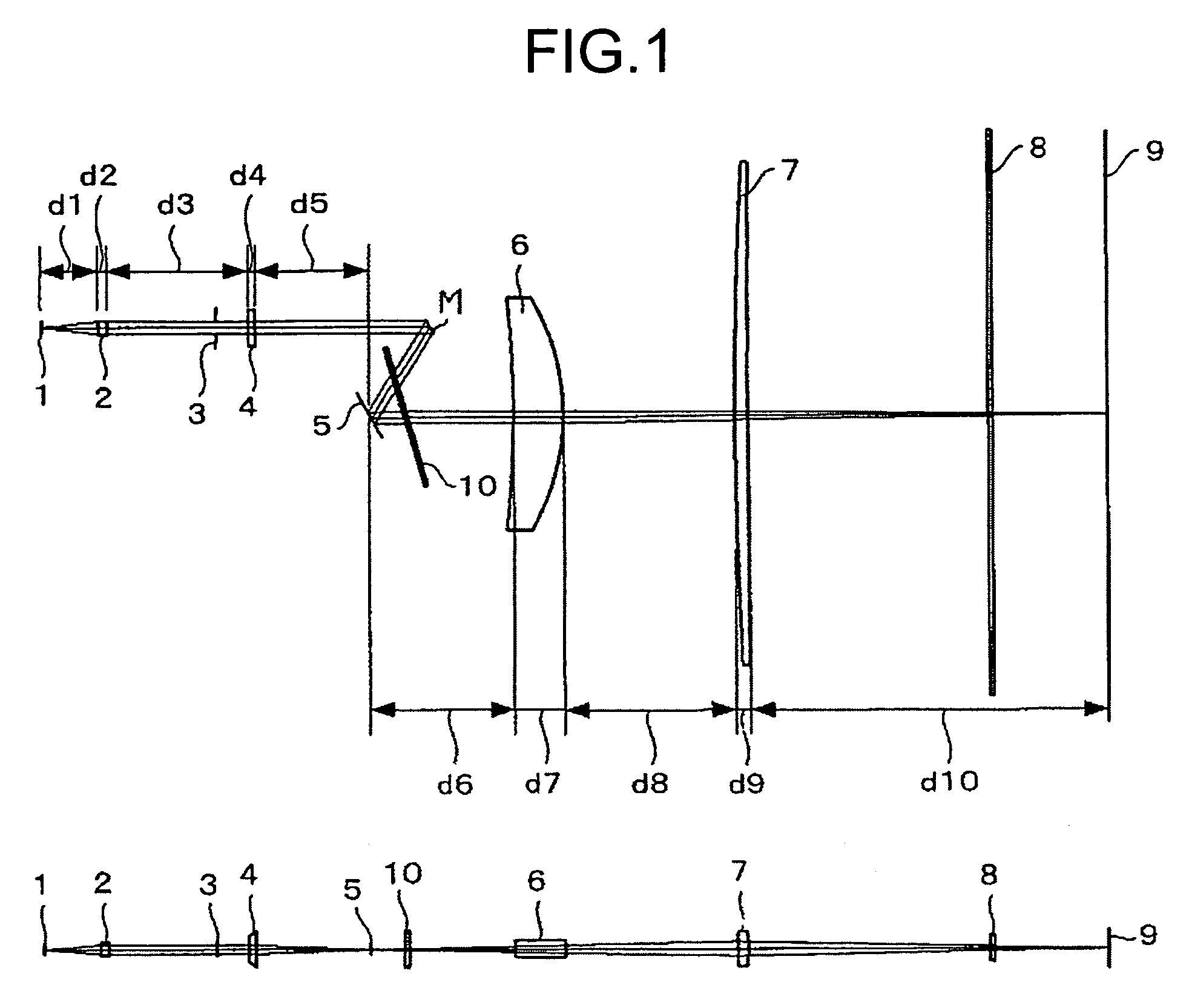
[0168]The first working example of the embodiment will be explained now. The emission wavelength of the light source is 655 nm at 25° C. and 659 mm at 45° C.

[0169]The characteristics of the coupling lens 2 are explained first. The incident surface is a diffractive surface having concentric circular gratings. Phase function φ(h) of the diffractive surface is represented by Expression (12).

φ(h)=C1·h2  (12)

where, h is the distance from the optical axis, C1 is a phase coefficient. The value of the phase coefficient, C1, is as follows:

[0170]C1=−1.127E−02.

[0171]The exit surface is an aspherical surface represented by Expression (7), the values of R, K, A4, A6, A8, and A10 are as follows:

[0172]R=−34.32864

[0173]K=−71.517137

[0174]A4=−0.208422E−03

[0175]A6=0.651475E−05

[0176]A8=−0.238199E−06

[0177]A10=0.770435E−08

[0178]The characteristics of the first lens 4″ will be explained now. The surface of the first lens 4 that faces toward the light source 1 is a plane surface in the main scanning direct...

second working example

[0262]The second working example of the embodiment will be explained now. The emission wavelength of the light source is 655 nm at 25° C. and 659 nm at 45° C.

[0263]The coupling lens 2 is made of glass. The incident surface of the coupling lens 2 is a plane surface and the exit surface is an aspherical surface represented by Expression (7). The shape of the exit surface of the coupling lens 2 is optimized so as to correct the wavefront aberration. The value of the paraxial curvature radius R is −18.49. The light beam emerging from the coupling lens 2 is virtually a parallel beam.

[0264]The characteristics of the first lens 4″ will be explained now. The incident surface of the first lens 4 is a toroidal surface having a curvature radius of −246.5 in the main scanning direction and −52.2 in the sub-scanning direction. The incident surface of the first lens 4 is a plane surface having an elliptical diffractive surface. The phase function φ(y,z) of the diffractive surface is represented b...

third working example

[0282]The second working example of the embodiment will be explained now. The emission wavelength of the light source is 655 nm at 25° C. and 659 nm at 45° C.

[0283]The coupling lens 2 is made of glass. The incident surface of the coupling lens 2 is a plane surface and the exit surface is an aspherical surface represented by Expression (7). The shape of the exit surface is optimized so as to correct the wavefront aberration. The value of the paraxial curvature radius R is the same as for the second working example, that is, −18.49. The light beam emerging from the coupling lens 2 is virtually a parallel beam.

[0284]The characteristics of the first lens 4″ will be explained now. The incident surface of the first lens 4 is a rotationally symmetrical spherical surface having a curvature radius of −246.5 with concentric diffraction gratings provided thereon as a diffractive surface. The diffractive surface is represented by Expression (12) in terms of its distance, h, from the optical axi...


PUM


Abstract

A first optical system guides a light beam from a light source to an optical deflector, and a second optical system converges the light beam deflected by the optical deflector on a surface to be scanned. The first optical system includes at least one resin lens having a diffractive surface. The second optical system includes at least one resin optical element. A beam diameter depth in a main scanning direction, Wm, that can have a maximum intensity of 1 / e2, satisfies conditionsΔm1+Δm2+Δm3−Δd1×(f2 / f1)2<Wm / 40  (1)Δd1>0 and Δm2<0.  (2)

Description

CROSS-REFERENCE TO RELATED APPLICATIONS[0001]The present document incorporates by reference the entire contents of Japanese priority document, 2004-284792 filed in Japan on Sep. 29, 2004, 2004-315996 filed in Japan on Oct. 29, 2004, 2005-031429 filed in Japan on Feb. 8, 2005, 2005-047314 filled in Japan on Feb. 23, 2005.BACKGROUND OF THE INVENTION[0002]1. Field of the Invention[0003]The present invention relates to an optical scanning device and an image forming apparatus.[0004]2. Description of the Related Art[0005]The recent years have seen advancement in high-density image formation through optical scanning in image forming apparatuses, such as digital copiers, laser printers, and the like. Also, there is a requirement for a smaller beam spot on the photosensitive drum and, from the point of view of overall cost reduction of the optical scanning device, use of a resin lens.[0006]On the other hand, any variation in environmental temperature brings about a variation in the curvatur...

Claims


Application Information

Patent Timeline
Patent Type & Authority Patents(United States)
IPC IPC(8): G02B26/08G02B3/08
CPCG02B7/008G02B26/124G02B26/125G02B27/0031G02B19/0014G02B27/4227G02B27/4283G02B19/0057G02B27/4211
Inventor HAYASHI, YOSHINORIUEDA, TAKESHISAKAI, KOHJI
Owner RICOH KK
Why Eureka
Try Eureka