Semiconductor laser element having tensile-strained quantum-well active layer

a quantum-well active layer, semiconductor laser technology, applied in the direction of lasers, semiconductor lasers, active medium materials, etc., can solve the problems of deterioration of the characteristics of the semiconductor laser, plastic fibers, and large internal loss, so as to reduce the threshold value, suppress the loss of mirrors, and achieve the effect of reducing the threshold valu

Inactive Publication Date: 2008-04-22
FUJIFILM HLDG CORP +1
View PDF3 Cites 0 Cited by
  • Summary
  • Abstract
  • Description
  • Claims
  • Application Information

AI Technical Summary

Benefits of technology

[0011]The object of the present invention is to provide a semiconductor laser element which has an oscillation wavelength of 645 to 650 nm at the room temperature (about 25° C.) and exhibits satisfactory current-optical output and lifetime characteristics.
[0016]Since the InGaP quantum-well active layer in the semiconductor laser element according to the present invention has a tensile strain, the semiconductor laser element benefits from the effect of the strain, which reduces the threshold value. In addition, the thickness of the InGaP quantum-well active layer is at least 10 nanometers, which is necessary for ensuring the reliability, is secured. Further, the mirror loss is suppressed by controlling the resonator length and the reflectances at the end facets. Therefore, the oscillation at the short wavelengths is realized without deterioration of the laser characteristics.
[0017]In particular, in the case where the oscillation wavelength λ of the semiconductor laser element is 645 to 650 nm at the ambient temperature of 25° C. when the optical output power of the semiconductor laser element is 1 mW, and the semiconductor laser element is used as a light source for optical communication, it is possible to suppress the internal loss in the optical fiber, and reduce the cost of placement of fibers. Thus, the present invention can contribute to the development of the optical networks.

Problems solved by technology

However, the plastic fibers cause great internal loss.
However, when the oscillation wavelengths of semiconductor lasers are decreased to 645 to 650 nm, the characteristics of the semiconductor lasers deteriorate due to various constraints.
Therefore, the semiconductor lasers having an oscillation wavelength of 645 to 650 nm are not yet practicable.
However, since it is impossible to obtain sufficient gain when the thickness of the quantum-well active layer is small, it is necessary to compensate for the insufficiency of the gain by increasing the number of quantum wells.
Therefore, it is impossible to secure sufficient reliability.
Nevertheless, since, in such a case, the thickness of the quantum-well active layer is near to the atomic sizes, it is difficult to control the thickness, and resultantly the oscillation wavelengths of individual semiconductor laser elements can greatly vary.
However, in this case, it is impossible to obtain a satisfactory current-optical output characteristic since the effect of reducing the threshold value in the strained quantum-well structure is lost.

Method used


Image

  • Semiconductor laser element having tensile-strained quantum-well active layer
  • Semiconductor laser element having tensile-strained quantum-well active layer
  • Semiconductor laser element having tensile-strained quantum-well active layer

Examples


Embodiment Construction

[0023]An embodiment of the present invention is explained in detail below with reference to drawings.

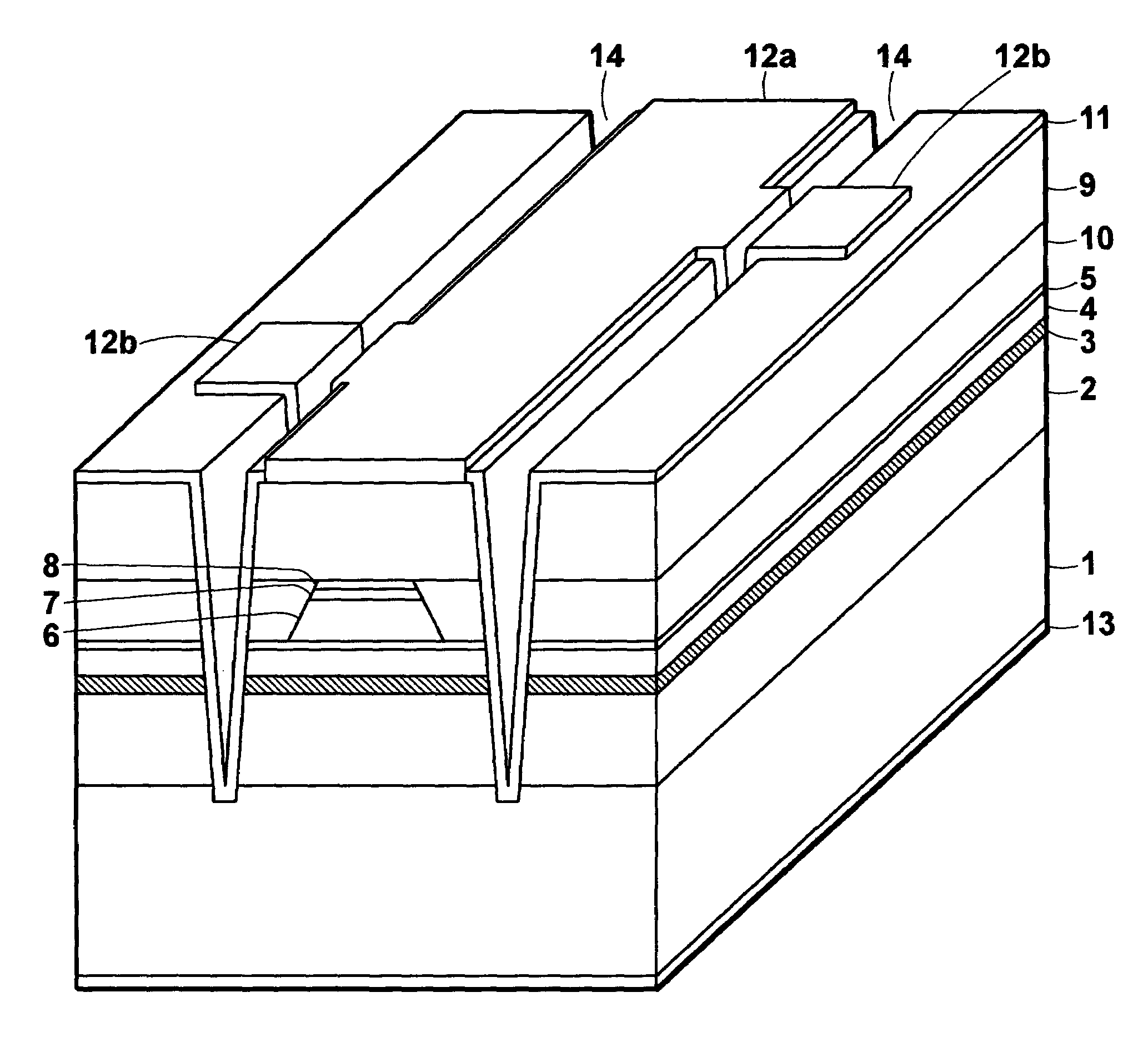
[0024]FIG. 1 is a schematic perspective view of the semiconductor laser element according to the embodiment of the present invention.

[0025]The semiconductor laser element according to the present embodiment is produced by forming a laser structure on an n-type GaAs substrate 1 having a principal plane the crystal orientation of which is tilted 15 degrees from (100) toward (011).

[0026]As illustrated in FIG. 1, the semiconductor laser element according to the present embodiment has a structure in which an n-type (AlxGa1-x)0.5In0.5P lower cladding layer 2 (x=0.7), a light-emission layer 3, a p-type (AlxGa1-x)0.5In0.5P first upper cladding layer 4 (x=0.7), and a p-type InGaP etching-stop layer 5 are formed in this order on the n-type GaAs substrate 1. It is preferable that the p-type InGaP etching-stop layer 5 is a tensile-strain InGaP layer so that the waveguide loss is reduced.

[0027]Fu...


PUM


Abstract

In a semiconductor laser element, a lower cladding layer of AlGaInP of the first conductive type, a lower optical waveguide layer of AlGaInP, a quantum-well active layer of InGaP, an upper optical waveguide layer of AlGaInP, and an upper cladding layer of AlGaInP of the second conductive type are formed in this order on a substrate of GaAs of the first conductive type. The degree of mismatch Δa / a with the substrate and the thickness dw of the quantum-well active layer satisfy the conditions, −0.6%≦Δa / a≦−0.3% and 10 nm≦dw≦20 nm. In addition, the resonator length Lc and the reflectances Rf and Rr of the opposite end facets satisfy the conditions, Lc≧400 μm and Rf×Rr≧0.5.

Description

BACKGROUND OF THE INVENTION[0001]1. Field of the Invention[0002]The present invention relates to a semiconductor laser element which is suitable for use in optical communications.[0003]2. Description of the Related Art[0004]In recent years, extension of optical fibers to individual homes has been becoming more prevalent, and the individual homes have been more intellectually empowered through optical networks. Although the transmission rates of the optical-fiber communications are currently about 100 Mbps, demands for transmission of greater amount of information at higher transmission rates will increase in the future.[0005]In the above circumstances, it is important to suppress the cost of placement of optical fibers. Therefore, attention is currently being focused on the plastic fibers rather than the quartz-based fibers, which are currently mainstream, since the plastic fibers are less expensive. In addition, since the plastic fibers have large core diameters and are easy to cou...

Claims


Application Information

Patent Timeline
Patent Type & Authority Patents(United States)
IPC IPC(8): H01S5/00H01L29/06H01S5/22H01S5/323
CPCB82Y20/00H01S5/3403H01S5/34326H01S5/0287H01S5/06226H01S5/1039H01S5/2222H01S5/2231
Inventor ASANO, HIDEKI
Owner FUJIFILM HLDG CORP
Why Eureka
Try Eureka