Gallium nitride material structures including substrates and methods associated with the same

a technology of gallium nitride and substrate, which is applied in the direction of semiconductor/solid-state device manufacturing, electrical apparatus, semiconductor/solid-state device manufacturing, etc., can solve the problems of defects, cracks, and difficulty in growing layers suitable for certain applications, and achieve the effect of avoiding dislocation, cracking and cracking

Active Publication Date: 2008-04-29
MACOM TECH SOLUTIONS HLDG INC
View PDF88 Cites 54 Cited by
  • Summary
  • Abstract
  • Description
  • Claims
  • Application Information

AI Technical Summary

Problems solved by technology

However, differences in the properties between gallium nitride materials and substrate materials can lead to difficulties in growing layers suitable for certain applications.
These differences in thermal expansion and lattice constant may lead to the formation of defects (e.g., dislocations) and cracking, as well as warping (e.g., bowing) of the overall structure.

Method used


Image

  • Gallium nitride material structures including substrates and methods associated with the same
  • Gallium nitride material structures including substrates and methods associated with the same
  • Gallium nitride material structures including substrates and methods associated with the same

Examples


example

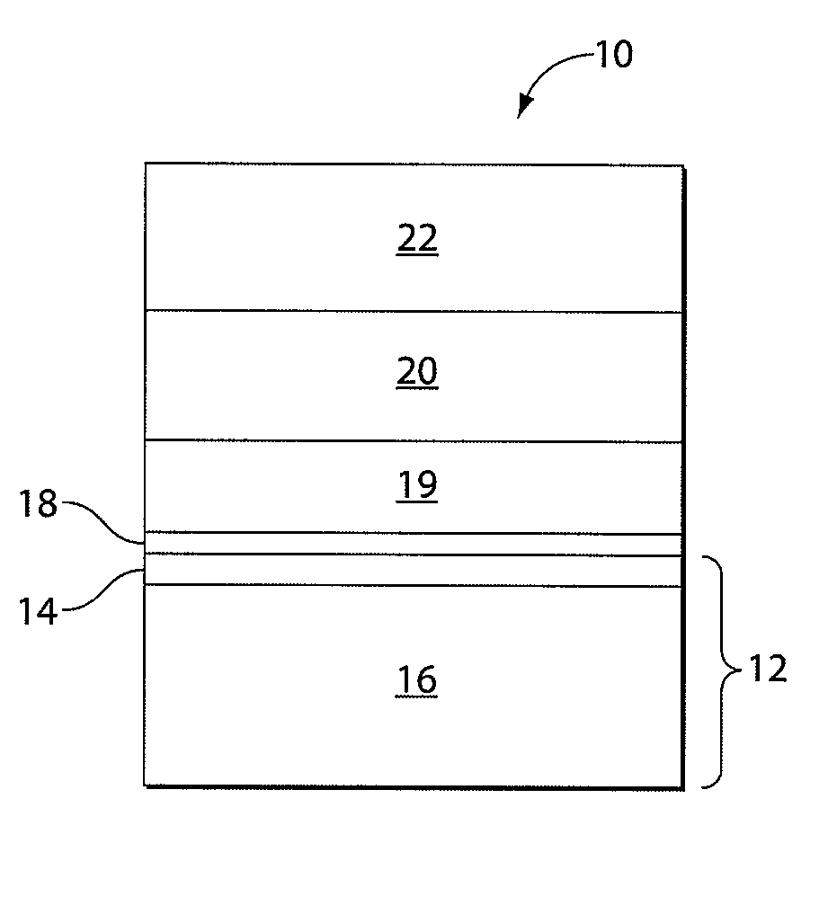
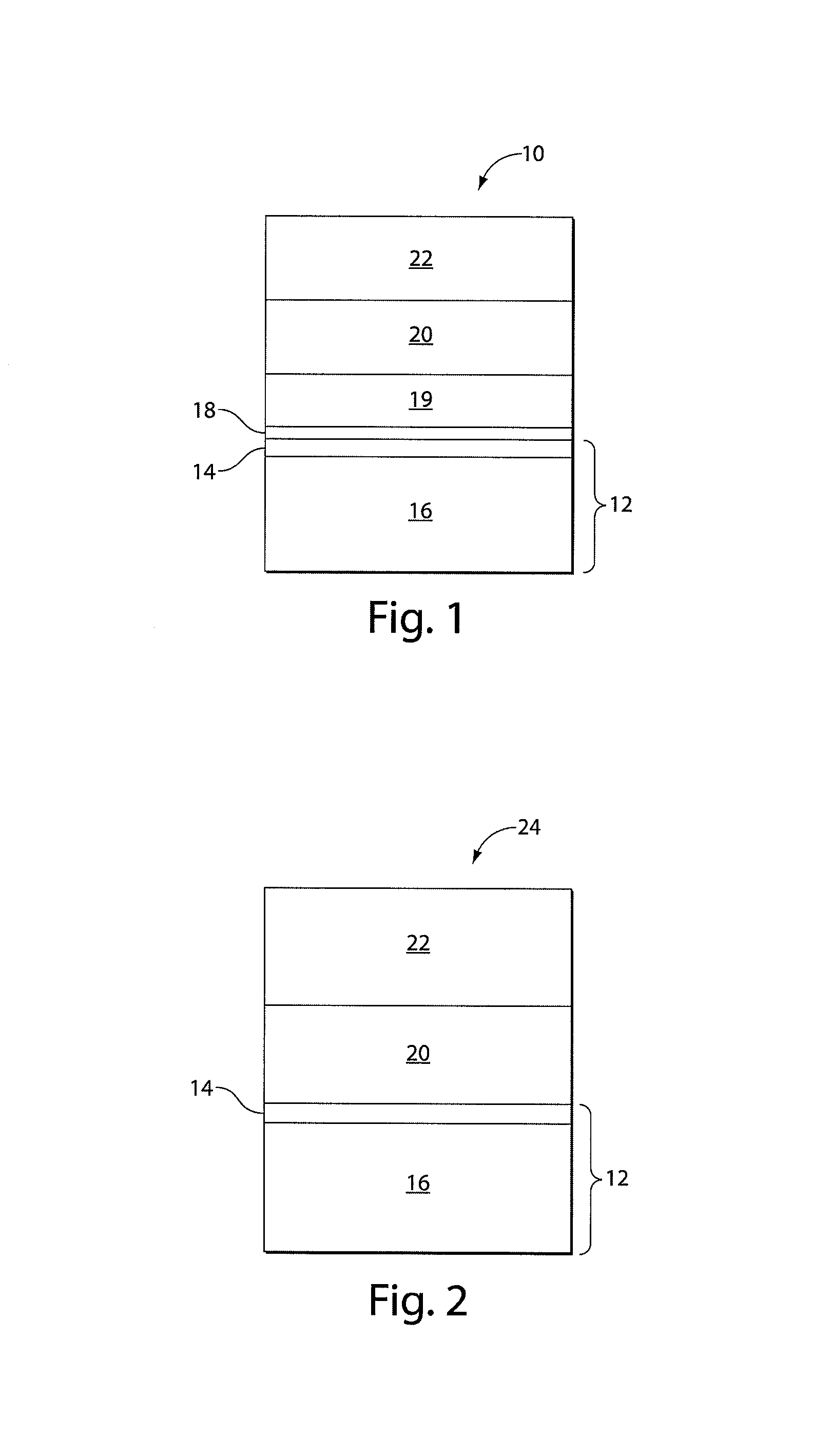
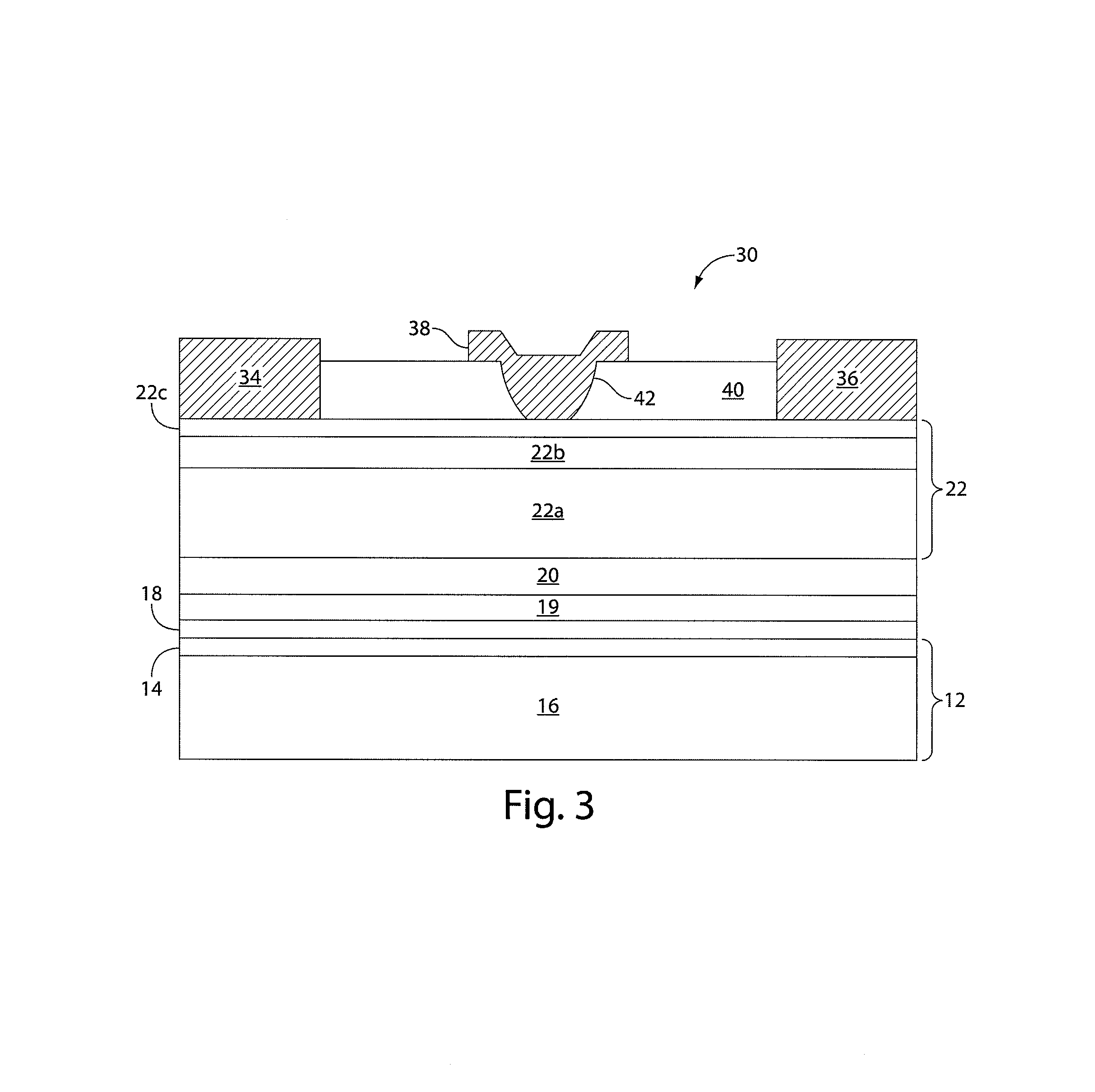
[0095]This example illustrates formation of a gallium nitride material-based structure including a composite substrate and characterization of the structure.

[0096]A gallium nitride-based structure was produced. The structure included a composite substrate (100 mm diameter) which comprised a 2 micron Si (111) surface layer formed on a poly SiC lower portion. The structure included a very thin (e.g., less than 50 Angstroms) amorphous silicon nitride-based strain absorbing layer formed on the composite substrate and a compositionally-graded AlxGa1-xN transition layer (including steps of AlN, Al0.6Ga0.4N, and Al0.3Ga0.7N) formed on the strain absorbing layer; and, a crack-free gallium nitride material region formed on the transition layer. The gallium nitride material region comprised a GaN buffer layer (thickness=1.65 micron) and an Al0.2Ga0.8N device layer (thickness=0.03 micron). The total thickness of the gallium nitride material region was about 1.7 micron. The structure was furthe...


PUM

PropertyMeasurementUnit
diameteraaaaaaaaaa
thicknessaaaaaaaaaa
thicknessaaaaaaaaaa

Abstract

Gallium nitride material-based semiconductor structures are provided. In some embodiments, the structures include a composite substrate over which a gallium nitride material region is formed. The gallium nitride material structures may include additional features, such as strain-absorbing layers and / or transition layers, which also promote favorable stress conditions. The reduction in stresses may reduce defect formation and cracking in the gallium nitride material region, as well as reducing warpage of the overall structure. The gallium nitride material-based semiconductor structures may be used in a variety of applications such as transistors (e.g. FETs) Schottky diodes, light emitting diodes, laser diodes, SAW devices, and sensors, amongst others devices.

Description

FIELD OF INVENTION[0001]The invention relates generally to gallium nitride materials and, more particularly, to gallium nitride material structures including substrates, as well as methods associated with the same.BACKGROUND OF INVENTION[0002]Gallium nitride materials include gallium nitride (GaN) and its alloys such as aluminum gallium nitride (AlGaN), indium gallium nitride (InGaN), and aluminum indium gallium nitride (AlInGaN). These materials are semiconductor compounds that have a relatively wide, direct bandgap which permits highly energetic electronic transitions to occur. Such electronic transitions can result in gallium nitride materials having a number of attractive properties including the ability to efficiently emit blue light, the ability to transmit signals at high frequency, and others. Accordingly, gallium nitride materials are being widely investigated in many microelectronic applications such as transistors, field emitters, and optoelectronic devices.[0003]In many ...

Claims


Application Information

Patent Timeline
Patent Type & Authority Patents(United States)
IPC IPC(8): H01L31/0328
CPCH01L21/0237H01L21/02381H01L21/02458H01L21/02488H01L21/02513H01L21/0254H01L29/267H01L29/66462H01L29/7783H01L29/2003
Inventor PINER, EDWIN L.RAJAGOPAL, PRADEEPROBERTS, JOHN C.LINTHICUM, KEVIN J.
Owner MACOM TECH SOLUTIONS HLDG INC
Why Eureka
Try Eureka