Field emission display device
a display device and field emission technology, applied in the field of image display devices, can solve the problems of difficult condition establishment and difficult control, and achieve the effect of wide and accurate adjustment of screen brightness, adversely affecting hue and contras
- Summary
- Abstract
- Description
- Claims
- Application Information
AI Technical Summary
Benefits of technology
Problems solved by technology
Method used
Image


Examples
first embodiment
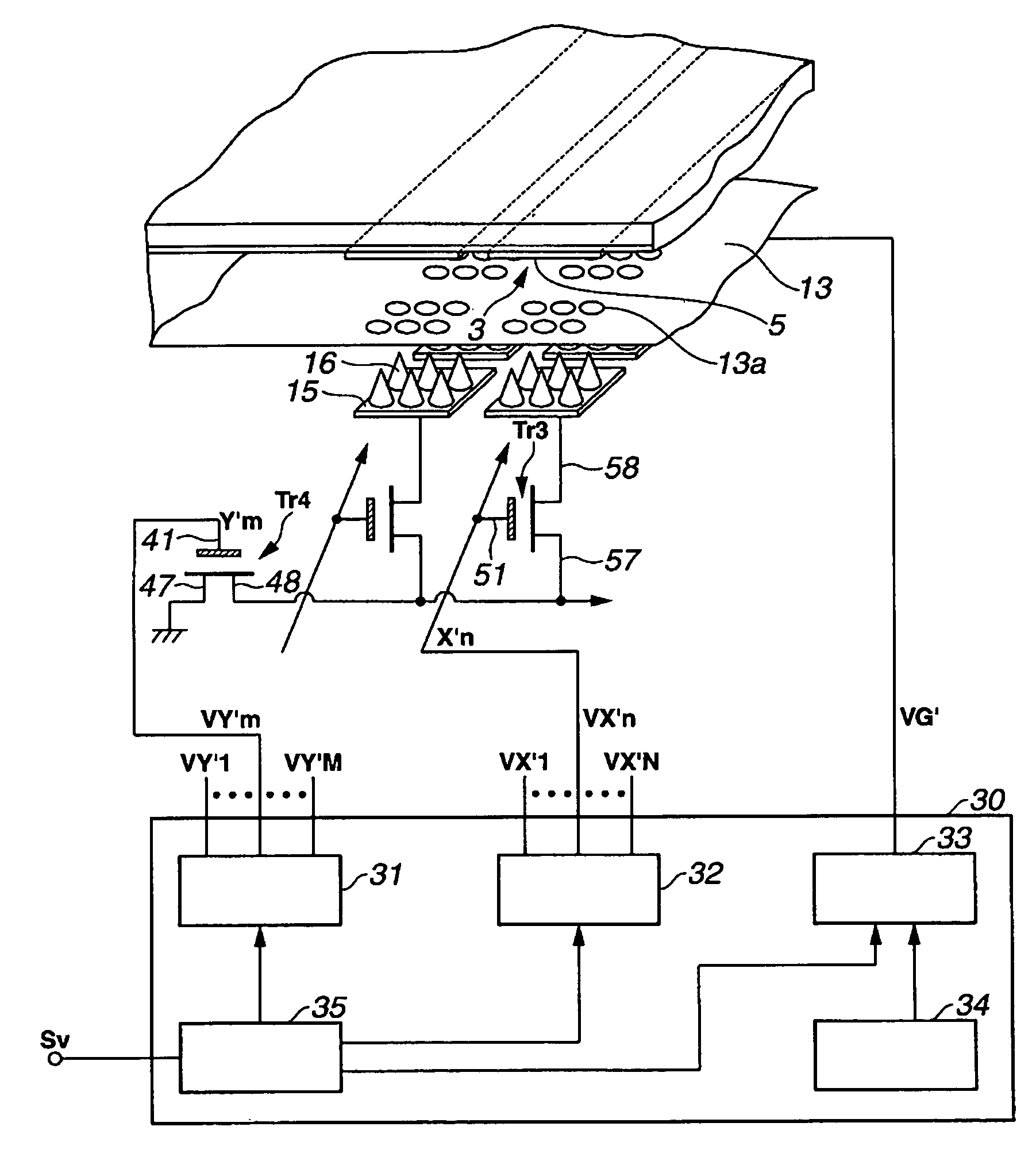
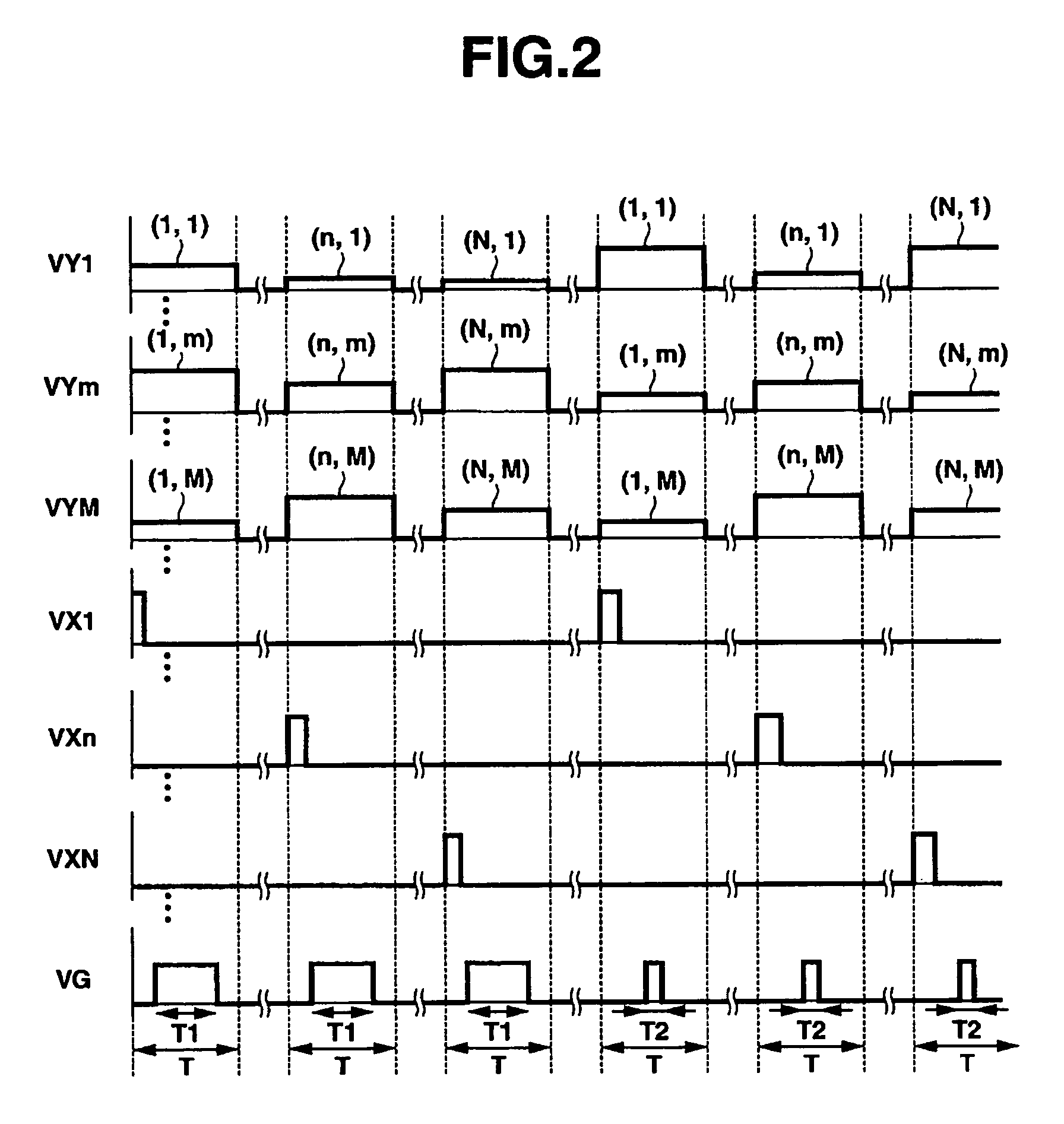
[0047]The waveform of a voltage applied to the gate electrode 13 in the first embodiment is a repetitive waveform, similar to that in other embodiments to be described later. That is, a voltage applied to the gate electrode 13 is set to a constant value enabling field emission for a period during one cycle. A voltage disenabling field emission is applied to the gate electrode 13 for the remaining period during the cycle. With one cycle defined as a ratio of 1, the time ratio Du ranges from 0 to 1. That is, during a time corresponding to the time ratio Du, or during a time represented by the product of one cycle time multiplied by the time ratio Du, the voltage applied to the gate electrode 13 allows the emitters 16 to generate the field emission. During the remaining period in one cycle, the voltage applied to the gate electrode 13 is set to suppress the field emission from the emitter 16. In the first embodiment, when the time ration is 1, voltages from VY1 to VYM, which make a lum...
second embodiment
Alteration of Second Embodiment
[0053]In the adjustment of the time ratio Du, an operator of the image display device may manually control the time ratio Du to obtain desired image brightness. However, the time ratio Du may be controlled in various other methods. For example, the time ratio Du of the voltage VG is controlled with the first gate control signal from the signal separation / drive signal generator 25. The optical sensor 24 detects the ambient brightness. The voltage VG may be controlled using the second gate control signal based on information from the optical sensor 24. Alternatively, the voltage VG may be controlled with the first gate control signal and the time ratio Du may be controlled with the second gate control signal. Thus, the control of voltage Vg may be performed together with the control of time ratio DU.
third embodiment
[0054]The signal separation / drive signal generator 25 includes a RAM (Random Access Memory) (not shown). The signal separation / drive signal generator 25 can absorb variations in the current Ia, flowing through the anode electrode 3, with respect to the voltage VY, for each cathode electrode 15. As shown in FIG. 3, the relationship between the current Ia and the voltage VY is linear. The voltages VYt, VYb, and VYw fluctuate, respectively. That is, the shape of the characteristic curve, shown in FIG. 3, depends on every cathode electrode 15. Therefore, even if the variation width of the current Ia with respect to the voltage VY is equalized to some extent in the narrow region, it is very difficult to equalize the characteristics in all regions using the RAM. In the present embodiment, variations in structure of the transistors Tr1 and Tr2, the capacitor 12, and the emitter 16 disposed on the cathode electrode and variations of the fluorescent substance layer 5 are absorbed using the R...
PUM
 Abstract
Description
Claims
Application Information
 - R&D
- Intellectual Property
- Life Sciences
- Materials
- Tech Scout
- Unparalleled Data Quality
- Higher Quality Content
- 60% Fewer Hallucinations
Browse by: Latest US Patents, China's latest patents, Technical Efficacy Thesaurus, Application Domain, Technology Topic, Popular Technical Reports.
© 2025 PatSnap. All rights reserved.Legal|Privacy policy|Modern Slavery Act Transparency Statement|Sitemap|About US| Contact US: help@patsnap.com