Circuit and method for switching active loads of operational amplifier input stage

a technology of operational amplifiers and active loads, which is applied in the direction of dc-amplifiers with dc-coupled stages, amplifiers with semiconductor devices/discharge tubes, and different amplifiers. it can solve the problems of increased circuit noise, increased power consumption, and inoperable folded cascode circuits b>5/b>, and achieves a wide common mode voltage input range and minimum noise

Active Publication Date: 2008-05-20
TEXAS INSTR INC
View PDF23 Cites 24 Cited by
  • Summary
  • Abstract
  • Description
  • Claims
  • Application Information

AI Technical Summary

Benefits of technology

[0022]It is an object of the invention to provide an operational amplifier having a wide common mode voltage input range and also having minimum noise.
[0023]It is another object of the invention to provide an operational amplifier having a wide common mode voltage input range and also having low power consumption.
[0025]It is another object of the invention to provide an operational amplifier having a wide common mode voltage input range which operates with optimal current densities in the active load transistors in a folded cascode circuit to provide a high slew rate.
[0026]It is another object of the invention to provide an operational amplifier having a wide common mode voltage input range which operates with optimal current densities in the active load transistors in a folded cascode circuit to provide fast recovery from overdrive conditions.
[0027]It is another object of the invention to provide an operational amplifier having a wide common mode voltage input range which operates with optimal current densities in the active load transistors in a folded cascode circuit so as to provide good rail-to-rail operation at low supply voltages.
[0028]It is another object of the invention to provide a fully differential operational amplifier having a wide common mode voltage input range while using gain boost circuitry on both sides of the folded cascode circuitry and nevertheless avoiding complexities associated with use of floating current sources of the kind described in commonly owned patent U.S. Pat. No. 6,150,883 in a fully differential operational amplifier.

Problems solved by technology

This causes folded cascode circuit 5 to become inoperative.
However, the above described large size of the active load transistors and large “idle” or bias current flowing through them results in a large “redundant” current flowing through folded cascode circuit 5, which is undesirable because that causes increased circuit noise and increased power consumption.
Use of large ratio current changes in the active load transistors necessitates use of large active load transistors, but this is undesirable because they have large transconductance (gm), which results in large input-referred noise.
In general, it is difficult optimize the design of a rail-to-rail folded cascode stage for switched input transistor pairs, especially for low voltage, low noise, low-power operation.
However, this approach presents difficulties in a fully differential operational amplifier if there is a need to include gain boost circuitry.
The described floating current sources tend to “tie up” one circuit node associated with the cascode transistors so as to not allow use of gain boost circuitry at that point without considerable additional circuit complexity.

Method used


Image

  • Circuit and method for switching active loads of operational amplifier input stage
  • Circuit and method for switching active loads of operational amplifier input stage
  • Circuit and method for switching active loads of operational amplifier input stage

Examples


Embodiment Construction

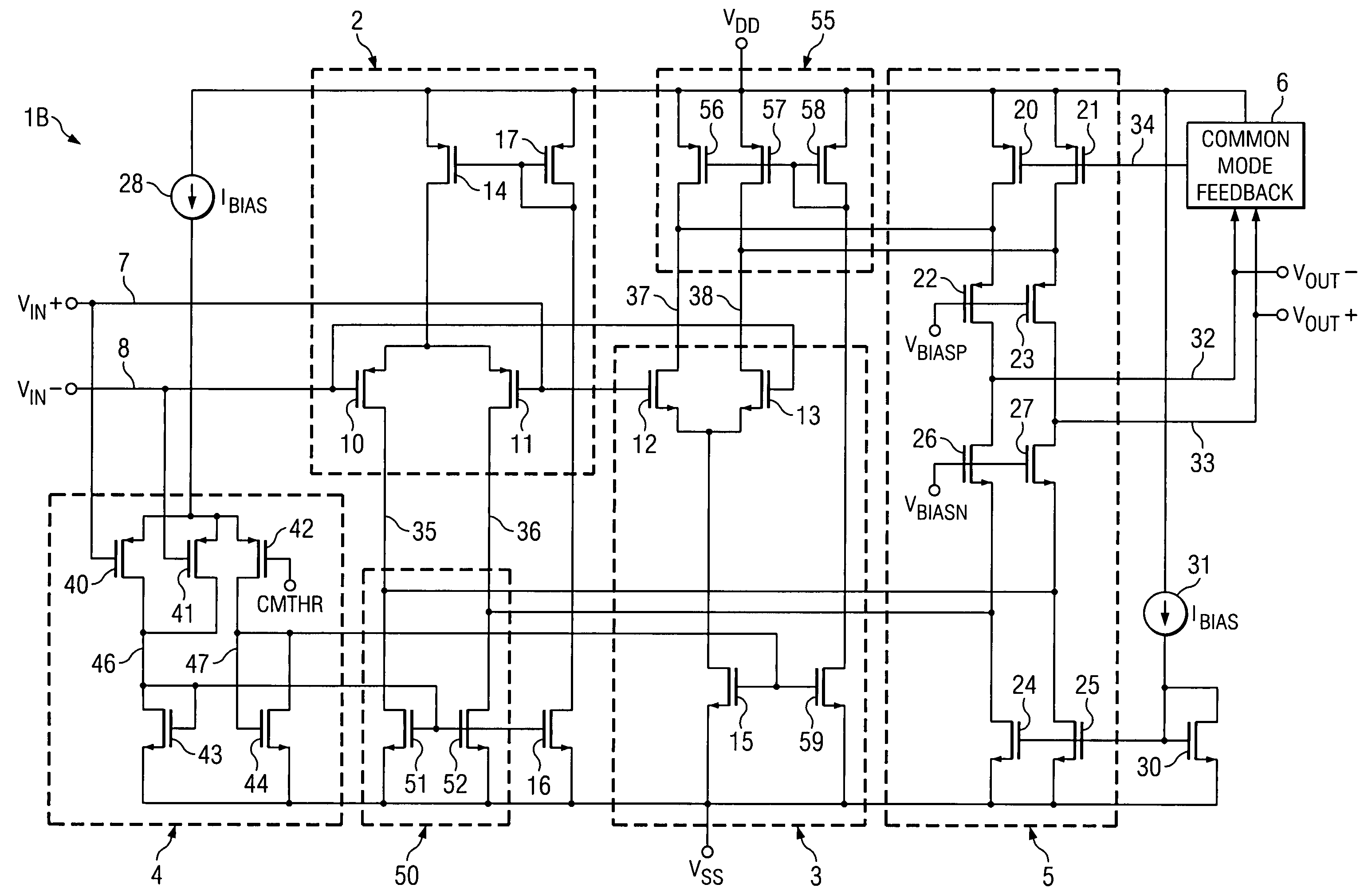
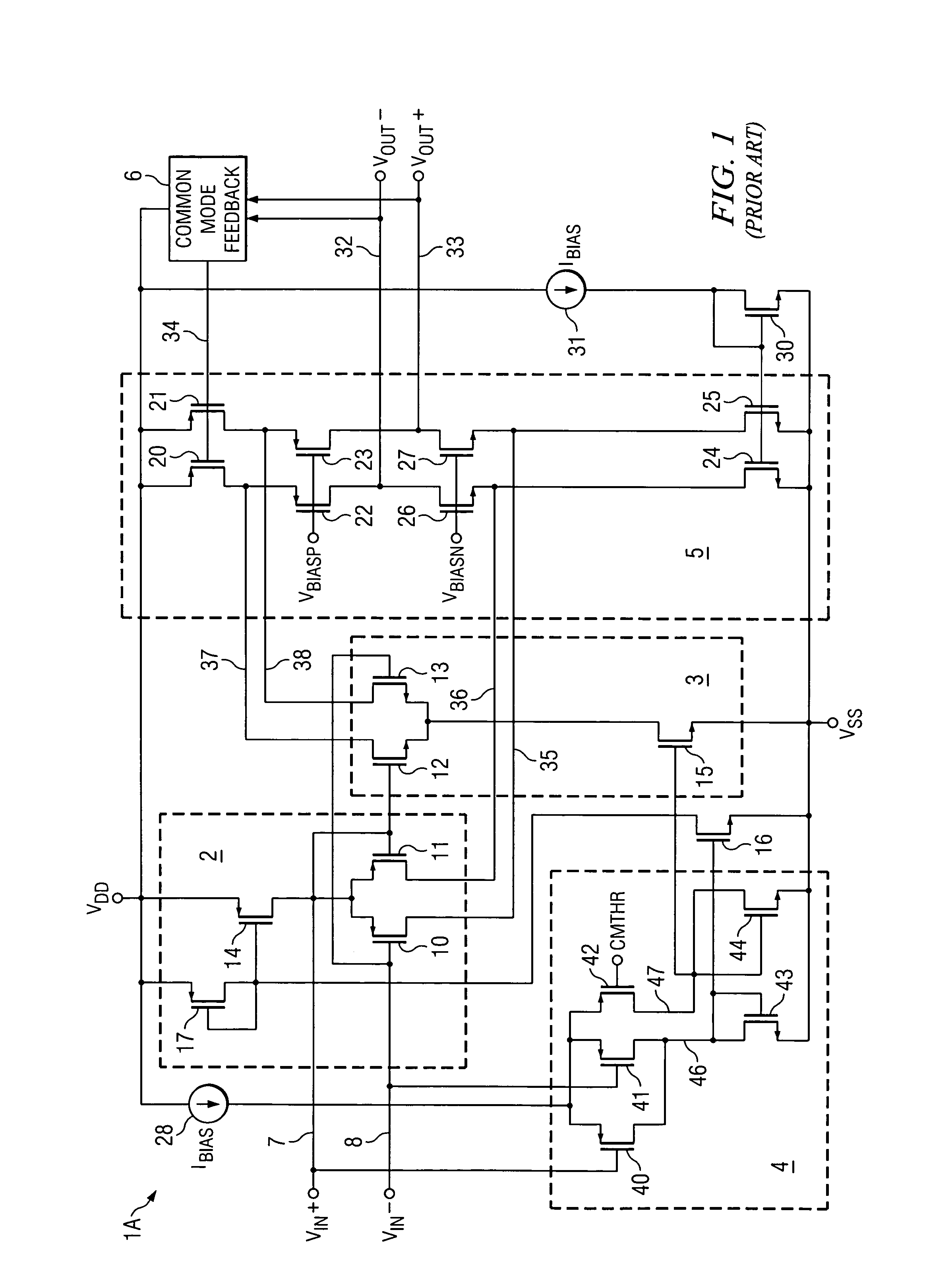
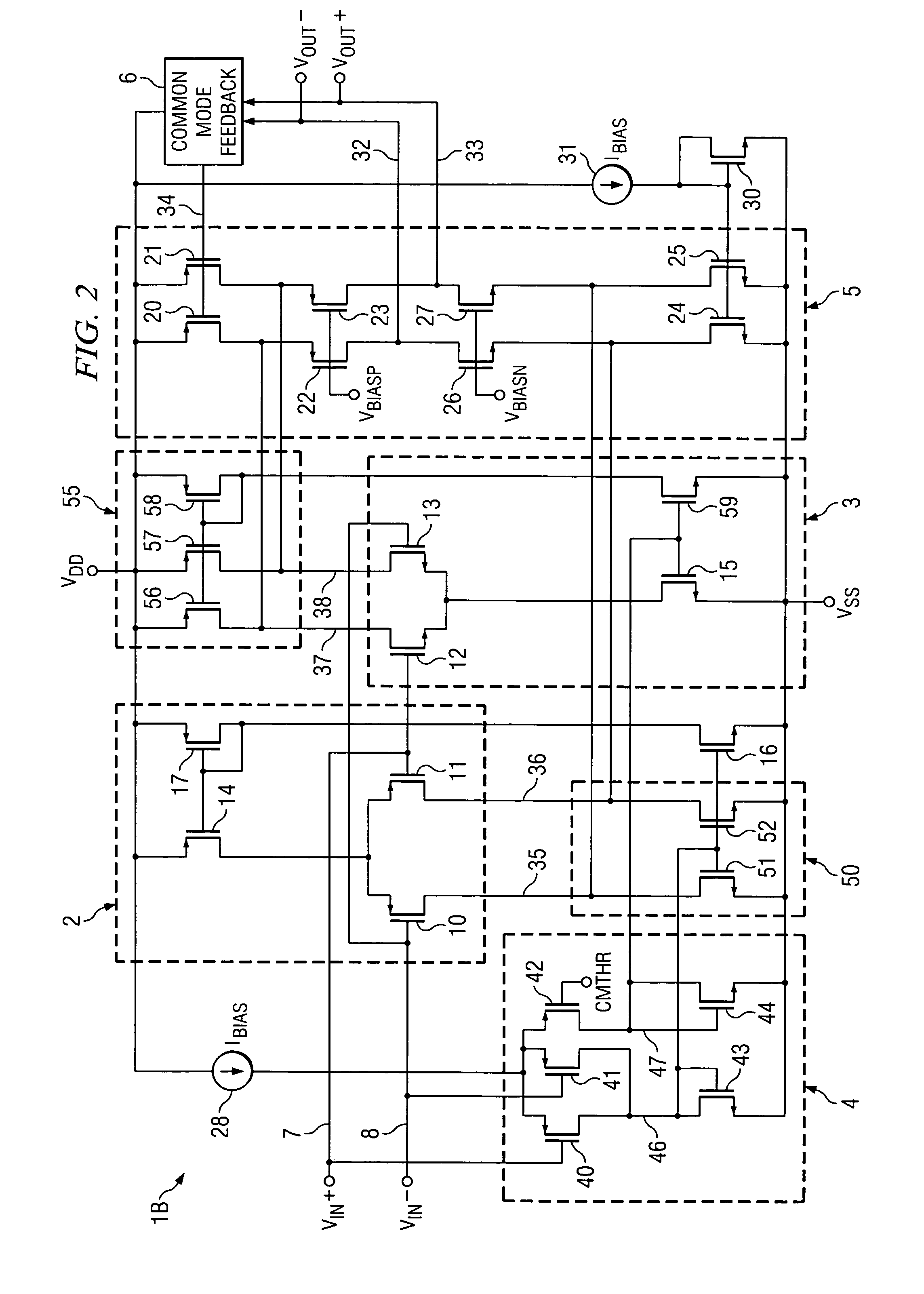
[0037]Referring to FIG. 2, operational amplifier 1B includes a low common mode voltage input stage 2 as in prior art FIG. 1, including source-coupled P-channel input transistors 10 and 11 and P-channel tail current transistor 14 connected to the sources of input transistors 10 and 11. The source of tail current transistor 14 is connected to VDD, and its gate is connected to the gate and drain of diode-connected P-channel transistor 17, the source of which is connected to VDD. Tail current transistor 14 is the output transistor of a controlled current mirror also including transistor 17. Operational amplifier 1B also includes high common mode voltage input stage 3 including source-coupled N-channel input transistors 12 and 13 and N-channel tail current transistor 15, which is one of the output transistors of a controlled current mirror including diode-connected N-channel transistor 44. The source of tail current transistor 15 is connected to VSS, and its gate is connected to the gate...


PUM


Abstract

An operational amplifier having a wide input common mode voltage range includes first (2) and second (3) differential input transistor pairs coupled to first (14) and second (15) tail current transistors. At least one of the first and second tail current transistor pairs is controlled by a common mode control circuit (4). A gate of the first tail current transistor (14) is coupled to the common mode control circuit (4) to turn the first tail current transistor on and to turn the second tail current transistor off when the common mode input voltage is below a common mode threshold voltage (CMTHR). A folded cascode stage (5) is driven by the first and second differential input transistor pairs. Switched active load transistors are coupled to active load transistors of the folded cascode stage and are operable in response to the common mode control circuit to divert part of a current produced by one of the first and second differential input pairs from the folded cascode circuit, depending on whether the common mode input voltage is above or below the common mode threshold voltage.

Description

BACKGROUND OF THE INVENTION[0001]The present invention relates generally to operational amplifiers having wide input common mode voltage range, and particularly to such operational amplifiers that include two differential input transistor pairs with “redirection” or “diverting” of tail currents from one input transistor pair to the other as the common mode voltage range changes, and more particularly to improvements which optimize current density in folded cascode circuit active load transistors so as to provide improved noise performance, improved power consumption, improved slew rate, improved overdrive recovery, and low-voltage rail-to-rail circuit operation.[0002]Operational amplifiers having wide input common mode voltage range frequently use two differential input transistor pairs of opposite conductivity type. For example, in one such operational amplifier one input transistor pair includes P-channel MOS input transistors or PNP input transistors and the other input transisto...

Claims


Application Information

Patent Timeline
Patent Type & Authority Patents(United States)
IPC IPC(8): H03F3/45
CPCH03F3/45219H03F2203/45424H03F2203/45504
Inventor TRIFONOV, DIMITAR T.ZHANG, JOY Y.
Owner TEXAS INSTR INC
Why Eureka
Try Eureka