Dual damascence process utilizing teos-based silicon oxide cap layer having reduced carbon content

a technology of teos and silicon oxide, applied in the direction of semiconductor/solid-state device manufacturing, basic electric elements, electric devices, etc., can solve the problem of worsening the problem of self-etching stop

Active Publication Date: 2008-05-27
UNITED MICROELECTRONICS CORP
View PDF1 Cites 17 Cited by
  • Summary
  • Abstract
  • Description
  • Claims
  • Application Information

AI Technical Summary

Benefits of technology

[0012]It is one object of the present invention to provide an improved copper dual damascene method, which is capable solving the above described via self-etching stop problem.

Problems solved by technology

This via self-etching stop problem becomes worse when the via opening is an isolated via.

Method used


Image

  • Dual damascence process utilizing teos-based silicon oxide cap layer having reduced carbon content
  • Dual damascence process utilizing teos-based silicon oxide cap layer having reduced carbon content
  • Dual damascence process utilizing teos-based silicon oxide cap layer having reduced carbon content

Examples


Embodiment Construction

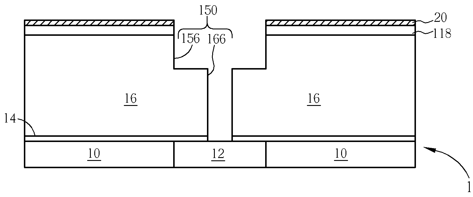
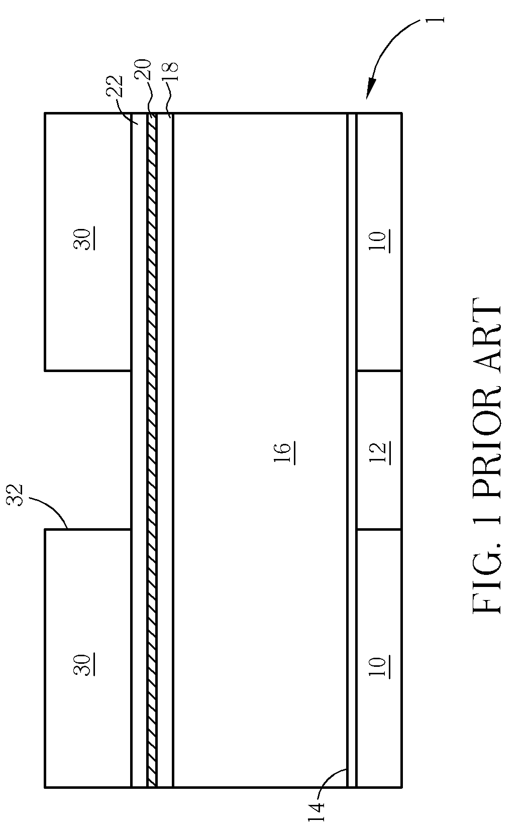
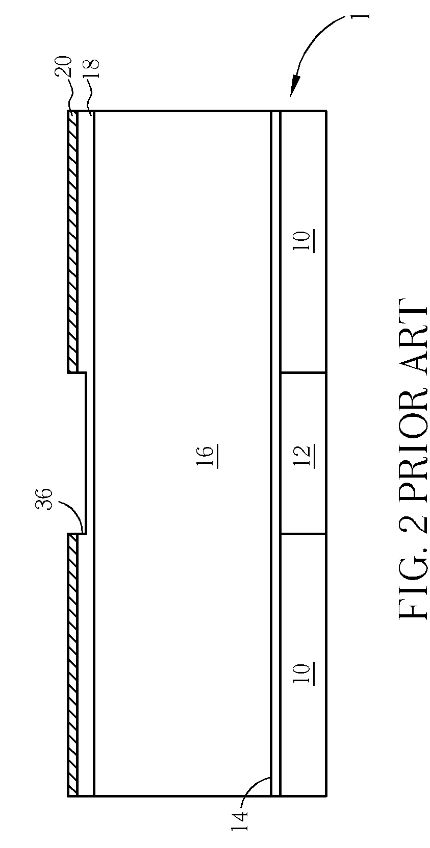
[0019]FIGS. 6-10 are schematic, cross-sectional diagrams showing a partial-via-first dual damascene process according to one preferred embodiment of this invention, wherein like numeral numbers designate like elements, regions or layers. As shown in FIG. 6, a substrate 1 having thereon a base layer or a lower low-k dielectric layer 10 is provided. Likewise, a lower copper wiring 12 is inlaid into the lower low-k dielectric layer 10. The lower copper wiring 12 and the low-k dielectric layer 10 are covered with a lower cap layer 14. According to the preferred embodiment, the lower cap layer 14 is made, for example, of nitrogen doped silicon carbide (SiCN) and has a thickness of about 300-800 angstroms, preferably about 500 angstroms.

[0020]Subsequently, a low-k dielectric layer 16, a TEOS-based silicon oxide cap layer 118, a metal hard mask layer 20 and a bottom anti-reflective coating (BARC) layer 22 are sequentially deposited on the lower cap layer 14. Preferably, the metal hard mask...


PUM

PropertyMeasurementUnit
thicknessaaaaaaaaaa
dielectric constantaaaaaaaaaa

Abstract

A dual damascene process starts with providing a substrate having thereon a base layer, a lower copper wiring inlaid into the base layer, and a lower cap layer covering the inlaid lower copper wiring. A dielectric layer is deposited on the lower cap layer. A TEOS-based oxide cap layer is deposited on the dielectric layer. The TEOS-based oxide cap layer has a carbon content lower than 1×10¹⁹ atoms / cm3. A metal hard mask is deposited on the TEOS-based oxide cap layer. A trench recess is etched into the metal hard mask and the TEOS-based oxide cap layer. A partial via feature is then etched into the TEOS-based oxide cap layer and the dielectric layer through the trench recess. The trench recess and partial via feature are etch transferred into the underlying dielectric layer, thereby forming a dual damascene opening, which exposes a portion of the lower copper wiring.

Description

BACKGROUND OF THE INVENTION[0001]1. Field of the Invention[0002]The present invention relates generally to copper interconnects. More particularly, the present invention relates to a partial-via-first copper dual damascene process utilizing a TEOS-based oxide cap layer having reduced carbon content, which is capable solving via self-etching stop problem.[0003]2. Description of the Prior Art[0004]Damascene interconnect processes incorporated with copper are known in the art, which are also referred to as “copper damascene processes” in the semiconductor industry. The copper damascene processes provide a solution to form a conductive wire coupled with an integral via plug without the need of dry etching copper. Either a single damascene or a dual damascene structure is used to connect devices and / or wires of an integrated circuit. Generally, the dual damascene process encompasses trench-first, via-first, partial-via-first, and self-aligned processes.[0005]FIGS. 1-5 are schematic, cros...

Claims


Application Information

Patent Timeline
Patent Type & Authority Patents(United States)
IPC IPC(8): H01L21/4763
CPCH01L21/7681H01L21/76829
Inventor CHEN, JEI-MINGLIN, MIAO-CHUNLAI, KUO-CHIHCHEN, MEI-LINGWENG, CHENG-MINGHUANG, CHUN-JENLAI, YU-TSUNG
Owner UNITED MICROELECTRONICS CORP
Why Eureka
Try Eureka